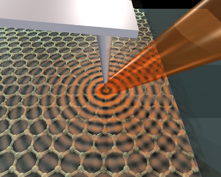
A multi-institute team of researchers has imaged and shown the propagation of surface plasmons on graphene using an infrared light beam and demonstrated a way to control them utilizing a basic electrical circuit.
 An infrared laser beam focused on the arm of an atomic-force microscope launches plasmons, waves through electrons, on the surface of graphene, a single honeycomb layer of linked carbon atoms. (credit: Basov Lab.)
The study results, reported online in the journal, Nature, will be helpful to use plasmons for processing and transmitting data in spaces that are too narrow to utilize light. The researchers made the devices by peeling graphene from graphite and rubbing it onto silicon dioxide chips.
The researchers then excited surface plasmons by illuminating the graphene surface with an infrared laser and utilized the atomic force microscope's ultrasensitive arm to measure the plasmonic waves. It was difficult to measure the outgoing waves. However, the waves reflected back when they reached the edge of the graphene. The reflected waves added to or cancelled out subsequent waves, generating a distinctive interference pattern that uncovers their amplitude and wavelength.
The research team demonstrated the possibility of modifying this pattern through controlling an electrical circuit comprising electrodes affixed to the graphene surface and a pure silicon layer under the chips.
First author, Zhe Fei informed that using light, the researchers excited £ 100-nm-length-scale surface plasmons that are capable of travelling at ultra speed from one end of the chip to the another end. The research team observed promising performance and these plasmon wavelengths are some of shortest calculated in any material, but the propagation of the waves is just as in metals such as gold. Moreover, unlike metal plasmons, graphene plasmons are tunable.
According to senior author, Dimitri Basov, graphene-based information processing and optoelectronics are highly potential fields. Plasmon study helps in learning the behavior of electrons in graphene and how basic interactions control their properties.