Norwegian University of Science and Technology (NTNU) researchers, Dr. Helge Weman and Professor Bjørn-Ove Fimland have developed a new technique to fabricate semiconductors from graphene.
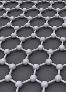
 Graphene comprises a single layer of carbon atoms. (illustration: Wikimedia Commons).
In this technique, a network of semiconductor nanowires is grown on graphene by bombarding its surface with arsenic molecules and gallium atoms. The resulting product is a 1-µm thick hybrid material that behaves as a semiconductor. By contrast, existing silicon semiconductors have several hundred folds thickness and their electrical conductivity gets affected by light, temperature or the inclusion of other atoms.
According to Weman, the ability to fabricate graphene-based semiconductors opens the door to produce more efficient and inexpensive semiconductor components when compared to existing silicon-based components. A material with a flexible and transparent base may transform the production of LED components and solar cells. Conventional windows in houses may also serve as television screens and solar panels. It may be possible to use mobile phone screens as a wrist watch.
Research Council's Clean Energy for the Future Programme funded the basic research that led to these breakthrough findings, while Nanotechnology and New Materials program that concluded recently had initiated the findings.
Nanowires on Graphene
The researchers have obtained support in securing patents and establishing a company from NTNU Technology Transfer, a joint partner to the program titled 'Commercialising R&D Results (FORNY2020) at the Research Council of Norway.' They will now start the production of prototypes for specific applications. Electronic giants like IBM and Samsung have been in touch with the researchers.
The research team believes that the new semiconductor hybrid materials will be commercially available within five years.