May 16 2013
Using a powerful combination of microanalytic techniques that simultaneously image photoelectric current and chemical reaction rates across a surface on a micrometer scale, researchers at the National Institute of Standards and Technology (NIST) have shed new light on what may become a cost-effective way to generate hydrogen gas directly from water and sunlight.*
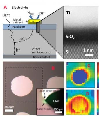
 Multiple views of NIST's photoelectrochemical hydrogen cell. Side schematic [A] shows princial components of the cell. Electrodes on the top are titanium toped with platinum. An incoming photon generates a electron (e) and hole (h). Microscope image [B] shows top of the cell surface with cylinderical electrodes and scanning laser beam. Photo-current scan [C] shows relatively high current around the base of the electrodes, while the electrochemical scan [D] shows a complex pattern of hydrogen generation on and around the electrode. (Credit: Esposito, Levin/NIST)
Their quarry is a potentially efficient, cost-effective, photoelectrochemical (PEC) cell—essentially a solar cell that produces hydrogen gas instead of electric current. "A major challenge with solar energy is dealing with solar intermittency," says NIST chemical engineer Daniel Esposito. "We demand energy constantly, but the sun's not always going to be shining, so there's an important need to convert solar energy into a form we can use when the sun's not out. For large-scale energy storage or transportation, hydrogen has a lot of benefits."
At its simplest, a PEC cell contains a semiconducting photoelectrode that absorbs photons and converts them into energetic electrons, which are used to facilitate chemical reactions that split water molecules into hydrogen and oxygen gases. It's not that easy. The best PEC cell has been demonstrated with an efficiency around 12.5 percent,** says Esposito. But, "it's been estimated that such a cell would be extremely expensive—thousands of dollars per square meter—and they also had issues with stability," he says. One big problem is that the semiconductors used to achieve the best conversion efficiency also tend to be highly susceptible to corrosion by the cell's water-based electrolyte. A PEC electrode that is efficient, stable and economical to produce has been elusive.
The NIST team's proposed solution is a silicon-based device using a metal-insulator-semiconductor (MIS) design that can overcome the efficiency/stability trade-off. The key is to deposit a very thin, but very uniform, layer of silicon dioxide—an insulator—on top of the semiconductor—silicon—that is well-suited for doing the photon-gathering work. On top of that is a polka-dot array of tiny electrodes consisting of platinum-covered titanium. The stable oxide layer protects the semiconductor from the electrolyte, but it's thin enough and transparent enough that the photons will travel through it to the semiconductor, and the photo-generated electrons will "tunnel" in the opposite direction to reach the electrodes, where the platinum catalyzes the reaction that produces hydrogen.
The MIS device requires good production controls—the oxide layer in particular has to be deposited precisely—but Esposito notes that they used fabrication techniques that are standard in the electronics industry, which has decades of experience in building low-cost, silicon-based devices.
To study the system in detail, the NIST team scanned the surface of the device with a laser beam, illuminating only a small portion at a time to record photocurrent with micrometer resolution. In tandem with the beam, they also tracked an "ultramicroelectrode" across the surface to measure the rate of molecular hydrogen generation, the chemical half of the reaction.*** The combination allowed them to observe two bonus effects of the MIS photoelectrode design: a secondary mechanism for hydrogen generation caused by the channeling of electrons through the oxide layer, and a more efficient transport of electrons to the reaction site than predicted.
The NIST team calculates an efficiency of 2.9 percent for their device, which also exhibits excellent stability during operation. While this efficiency is far lower than more costly designs, they note that it is 15 times better than previously reported results for similar silicon-based MIS devices, and the new data from their microanalysis of the system points towards several potential routes to improving performance. The detailed results are found in Nature Materials.
* D.V. Esposito, I. Levin, T.P. Moffat and A.A. Talin. H2 evolution at Si-based metal–insulator–semiconductor photoelectrodes enhanced by inversion channel charge collection and H spillover. Nature Materials. Published online, May 5, 2013. doi:10.1038/nmat3626.
** In the 90s by the U.S. Department of Energy's National Renewable Energy Laboratory.
*** Technically, scanning photocurrent microscopy (SPCM) and scanning electrochemical microscopy (SECM).