Feb 21 2018
Sheets of electrons with the ability to move rapidly in just two dimensions - termed 2D electron gas - have distinctive characteristics that can be tapped for high-speed and innovative electronic devices. Discovered in 2004, 2D electron gas has been investigated by scientists to observe the way it can be applied to devices such as actuators, superconductors, electronic memory devices, and so on.
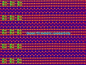 The scanning transmission electron micrograph shows that the atomic structure was alternately arranged in the three-layer and the zig-zag two-layer thick chain-like slabs, showing quasi-1D metallic conductivity in the former. (Image credit: Tohoku University)
Recently, scientists from Tohoku University in Japan worked with an international team of researchers and discovered the atomic structure of a class of perovskite-associated materials exhibiting intriguing 2D conductive characteristics.
The materials are formed of niobium, strontium, and oxygen atoms, and have a layered structure acquired from perovskite. Such strontium niobate compounds look propitious for developing state-of-the-art electronics due to their “quasi-one-dimensional” metallic conductivity.
Yuichi Ikuhara from Tohoku University’s Advanced Institute for Materials Research collaborated with Johannes Georg Bednorz from Zürich Research Laboratory and colleagues to use atom-resolved scanning transmission electron microscopy in combination with theoretical computations to understand the effect of the addition of oxygen atoms to strontium niobates on their conductivity. Based on the concentration of oxygen atoms, four different materials were formed.
The scientists discovered that three of the four materials conducted electricity, whereas the fourth one was an insulator. They found out that, at the atomic level, the materials included alternating chain-like and zigzag slabs. Based on the oxygen atom concentration, there were two, three, or four layers of chain-like slabs, at times differing within the same material. In all the materials, the zigzag slabs acted as insulating layers. However, the chain-like slabs acted as conducting layers only in three of the four materials.
The researchers ascertained that local electrical conductivity inside the material was directly related to the shapes of the niobate octahedra in the layers. Upon displacing the positive ions of niobium toward the niobate octahedra centers, a local conducting nature was activated.
In general, 2D conducting layers are developed by forming an interface between two insulators. At present, researchers should be in a position to attain the same objective by dividing 3D conducting materials into stacks of 2D conducting layers isolated by insulating layers, the scientists have stated in their work published in the ACS Nano journal. This could result in the application of the material in developing 2D electrical conducting materials and devices.