Feb 11 2019
For the first time, scientists have successfully imaged “edge conduction” in a recently discovered 2D quantum material and topological insulator called monolayer tungsten ditelluride, or WTe2.
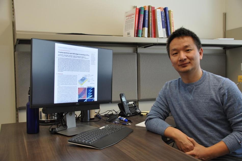
 Yongtao Cui is an assistant professor of physics and astronomy at UC Riverside. (Image credit: I. Pittalwala, UC Riverside.)
The research team included investigators at the University of California, Riverside (UCR) and the University of Washington. The latest study makes it feasible to manipulate this edge conduction aspect to develop electronic devices that are more energy efficient.
Electrical current flows everywhere in a standard conductor. By contrast, insulators do not conduct electricity readily. In a unique type of material called topological insulators, the interior acts as an insulator yet the boundaries of these kinds of materials are ensured to be conductive owing to its topological characteristics, thus leading to a feature known as “topological edge conduction.”
Topology refers to the mathematical analysis of the characteristics of a solid or geometric figure that remains unchanged by either bending or stretching. Utilizing this concept on electronic materials can result in the discovery of several interesting phenomena, for instance, topological edge conduction. Working just like highways for electrons, topological edge conduction channels enable electrons to pass with a minimal amount of resistance. In addition, since edge channels could be extremely narrow, it is possible to further miniaturize electronic devices.
The results of the study have been reported in Science Advances.
Several materials have been shown to be 3D topological insulators. But 2-D topological insulators are rare. Several recent experiments established that monolayer WTe2 is the first atomically thin 2D topological insulator.
Yongtao Cui, Study Lead and Assistant Professor, Department of Physics and Astronomy, University of California, Riverside
Cui elucidated that in the case of a 3D topological insulator, conduction occurs at its surfaces; such kinds of conducting features for a 2D sheet-like material simply lie at the sheet edges.
Cui’s laboratory applied an innovative experimental method known as microwave impedance microscopy, or MIM in short, for directly imaging the conduction at the edges of the monolayer WTe2 material.
“Our results unambiguously confirm edge conduction in this promising material,” stated Cui.
While WTe2 has been in existence for many years, this material started to attract interest only in the last several years because of its unique electronic and physical characteristics discovered through topological physics. Layers of WTe2 are stacked together through van der Waals interactions and can be effortlessly exfoliated into thin, 2D, sheets resembling graphene.
In addition to conduction at the edges in monolayer WTe2, we also found that the conductive channels can extend to the interior of the material, due to imperfections—such as cracks. Our observations point to new ways to control and engineer such conduction channels via mechanical or chemical means.
Yongtao Cui, Study Lead and Assistant Professor, Department of Physics and Astronomy, University of California, Riverside
The monolayer WTe2 samples were prepared by Cui’s collaborators at the University of Washington. At UCR, Cui’s laboratory carried out the MIM measurement, in which a microwave electrical signal is sent to a sharp metal tip, and the tip is positioned close to the monolayer WTe2 surface. Resolving the microwave signal reflected back by the sample could allow the scientists to establish whether the sample region, which is directly beneath the tip, was conductive or not.
“We scanned the tip across the entire sample and directly mapped the local conductivity,” stated Cui “We performed all the measurements at cryogenic temperatures, needed for monolayer WTe2 to exhibit the topological property. The topological properties of monolayer WTe2 can potentially serve as a platform to realize essential operations in quantum computing.”
Cui’s laboratory is already investigating innovative ways to exploit the topological physics and edge conduction channels in the monolayer WTe2.
We are looking into whether stacking monolayer WTe2 with other 2-D materials can alter its topological property. We are also using mechanical and chemical methods to create networks of conduction channels. The MIM technique we used offers a powerful means to characterize the conduction channels in topological materials such as monolayer WTe2.
Yongtao Cui, Study Lead and Assistant Professor, Department of Physics and Astronomy, University of California, Riverside
In this research, Cui was joined by Yanmeng Shi, Ben Niu, and Brian A. Francisco of UCR; Joshua Kahn, Zaiyao Fei, Bosong Sun, Xinghan Cai, Xiaodong Xu, and David H. Cobden of the University of Washington; Di Wu of Nanjing University, China; and Zhi-Xun Shen of Stanford University; Shi, Kahn, and Niu are the paper’s co-first authors.
Cui’s startup funds supported the study performed at UCR.