Jul 25 2019
TU Wien researchers have achieved an important breakthrough in transistor technology: With the support of novel insulators, superior-quality transistors can be built using two-dimensional (2D) materials.
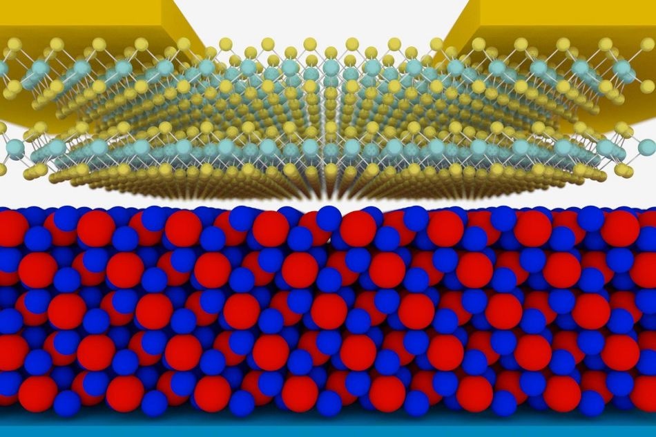
 Transistor—Schematics of the new transistor: the insulator in red and blue, and the semiconductor above (Copyright: TU Wien)
Over the years, the transistors on microchips have become faster, smaller, and cheaper. About every two years, the number of transistors on commercial chips has doubled—this occurrence became termed as “Moore’s Law.” But for many years now, Moore’s law is no longer valid. The miniaturization has attained a natural limit, as new issues crop up when a length scale of just a few nanometers is approached.
Now, however, the next big miniaturization step could quickly become possible—with so-called “two-dimensional (2D) materials” that may have just a single atomic layer. With the help of a novel insulator composed of calcium fluoride, researchers at TU Wien (Vienna) have developed an ultra-thin transistor, which has superior electrical properties and contrary to earlier technologies, can be miniaturized to a very small size.
The new technology has recently been described in the journal Nature Electronics.
Ultra-Thin Semiconductors and Insulators
Research on semiconductor materials necessary for the fabrication of transistors has seen substantial progress of late. Today, ultra-thin semiconductors can be composed of 2D materials, comprising just a few atomic layers.
But this is not enough to build an extremely small transistor. In addition to the ultra-thin semiconductor, we also need an ultra-thin insulator.
Tibor Grasser, Professor, Institute of Microelectronics, TU Wien
This is because of the basic design structure of a transistor: current can travel from one side of the transistor to the other, but only if a voltage is applied in the middle, forming an electric field. The electrode delivering this field has to be electrically insulated from the semiconductor itself.
There have already been transistor experiments with ultra-thin semiconductors, but until now they were coupled with ordinary insulators. There is not much benefit in reducing the thickness of the semiconductor when it still has to be combined with a thick layer of insulator material. There is no way of miniaturizing such a transistor any further. Also, at very small length scales the insulator surface turned out to disturb the electronic properties of the semiconductor.
Tibor Grasser, Professor, Institute of Microelectronics, TU Wien
Thus, Yury Illarionov, a postdoc in Tibor Grasser’s team, tried a new method. He used ultra-thin 2D-materials for both the semiconductor part of the transistor and the insulating part. By selecting ultra-thin insulating materials like ionic crystals, a transistor with a size of just a few nanometers can be constructed. The electronic properties are enhanced because ionic crystals can have a perfectly typical surface, without a single atom bulging from the surface, which could hamper the electric field.
“Conventional materials have covalent bonds in the third dimension—atoms that couple to the neighboring materials above and below,” explains Tibor Grasser. “This is not the case in 2D materials and ionic crystals, and so they do not interfere with the electrical properties of the semiconductor.”
The Prototype is a World Champion
To create the new ultra-thin transistor, calcium fluoride was chosen as the insulating material. The calcium fluoride layer was made at the Ioffe Institute in St. Petersburg, where the first author of the publication, Yury Illarionov, is formerly from before joining the team in Vienna. The transistor itself was then made by Prof. Thomas Müller’s team at the Institute of Photonics at TU Wien and examined at the Institute for Microelectronics.
The very first prototype already exceeded all expectations: “or years, we have received quite a number of different transistors to investigate their technical properties—but we have never seen anything like our transistor with the calcium fluoride insulator,” says Tibor Grasser. “The prototype with its superior electrical properties outshines all previous models.”
Now the researchers are keen to find out which groupings of insulators and semiconductors operate best. It may require a couple more years before the technology can be used for commercially available computer chips as the manufacturing processes for the material layers still need to be refined.
In general, however, there is no doubt that transistors made of 2D materials are a highly interesting option for the future. From a scientific point of view, it is clear that the fluorides we have just tested are currently the best solution for the insulator problem. Now, only a few technical questions remain to be answered.
Tibor Grasser, Professor, Institute of Microelectronics, TU Wien
This new type of smaller and faster transistor is likely to enable the computer industry to move the next level. In this manner, Moore’s law of exponentially increasing computer power could be revived soon.