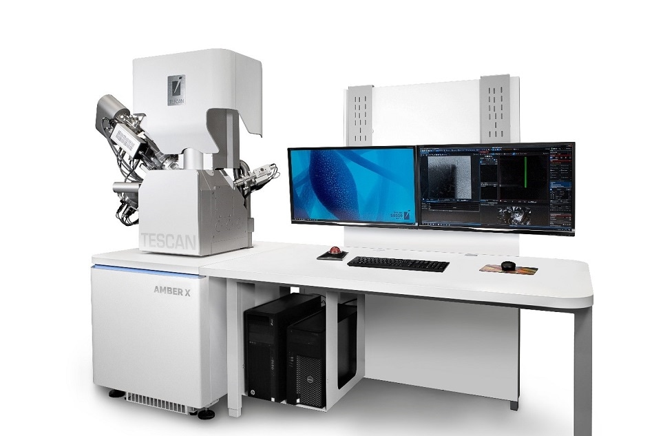
As the first SEM manufacturer to commercialize integrated xenon plasma FIB with the SEM, TESCAN proudly announces TESCAN AMBER X. TESCAN AMBER X is a new FIB-SEM solution that combines high throughput plasma-assisted ion milling with improved ultra-high resolution (UHR) field-free SEM optics, a combination ideally suited for materials characterization over a significantly wider sample range. TESCAN AMBER X target applications include milling and characterization of large cross-sections (up to 1 mm in width), multiscale, multi-modal FIB-SEM tomography, and contamination-free preparation of micro- and nano-structures for subsequent testing or characterization.
Whereas the more common gallium FIB-SEM systems, such as TESCAN AMBER or SOLARIS, remain the solution of choice for applications that require the highest ion beam milling precision, their versatility for multiscale characterization and sample preparation of novel materials can be compromised by their limited milling speed and liquid metal ion contamination artefacts. With TESCAN AMBER X, we propose a unique solution for materials laboratories that require multiscale characterization over the widest range of traditional and novel materials.
Jiri Dluhos, Product Manager, TESCAN FIB-SEM Solution Portfolio for Material Sciences
Xenon plasma FIB differs from Gallium liquid metal ion FIB technology with its ability to focus more ions into the beam, thereby achieving higher ion beam currents than what is possible with liquid metal ion species. The benefit of higher ion beam currents, up to 1 uA for TESCAN AMBER X’s high-resolution plasma FIB configuration, is their significantly higher milling rates — one order of magnitude and more – while also delivering fine milling and polishing capabilities with 15 nm optical resolution. And, due to the inert nature of xenon, plasma FIB eliminates any risk of sample contamination by ion implantation.
The field-free BrightBeam™ electron column of TESCAN AMBER X extends ultra-high resolution for concurrent SEM, EDS or EBSD characterization to a wider range of materials, like metallic, magnetic, non-conductive or beam-sensitive, that might otherwise be affected by non-field-free electron optics, while still achieving ultra-high resolution (1.5 nm @ 1 kV).
TESCAN AMBER X, based on the TESCAN S8000 platform, is available for order now, with first deliveries expected in the first quarter of 2020.