Feb 13 2020
Semiconductor devices and other similar microelectronics are at the core of the technologies used by people every day.
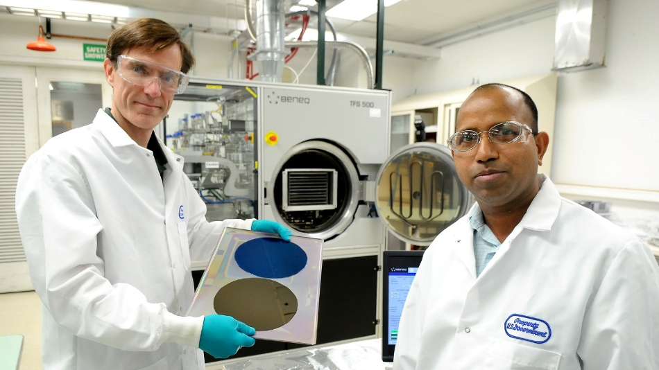
 Argonne chemists Jeff Elam (left) and Anil Mane (right) and colleagues have molecular layer etching that may help develop microelectronics and show the way beyond Moore’s Law. Not shown are Matthias Young, Angel Yanguas-Gil, Devika Choudhury and Steven Letourneau. Image Credit: Argonne National Laboratory.
As people move into a period where they are stretching the boundaries of Moore’s Law, it becomes necessary to explore new ways so that more circuitry can be continuously packed into individual devices to boost the capability and speed of computers.
At the U.S. Department of Energy’s (DOE) Argonne National Laboratory, scientists have come up with a novel method that can lead to the development of these progressively small but intricate devices. This method, called molecular layer etching, has been described in the latest paper published in the Chemistry of Materials journal.
To reduce the size of microelectronics, manufacturers have to insert an increasing amount of circuitry onto 3D structures and smaller films. Currently, this process is performed by using techniques like thin film deposition and etching to remove or grow films one layer at a time.
Our ability to control matter at the nanoscale is limited by the kinds of tools we have to add or remove thin layers of material. Molecular layer etching (MLE) is a tool to allow manufacturers and researchers to precisely control the way thin materials, at microscopic and nanoscales, are removed.
Matthias Young, Study Lead Author and Assistant Professor, University of Missouri
Young was also a former postdoctoral researcher at Argonne National Laboratory.
Along with the molecular layer deposition (MLD) method, another deposition technique called MLE can be utilized to design microscopic architectures. These methods are analogs of atomic layer etching (ALE) and atomic layer deposition (ALD) techniques, which are often used for producing microelectronics. But unlike atomic layering approaches, which only deal with inorganic films, MLE and MLD can also be used for growing or removing organic films.
How it Works
Theoretically, MLE works by subjecting thin films, which have a thickness of several micrometers or nanometers, to gas pulses within a vacuum chamber. The process begins with one gas (Gas A), which enters the chamber and immediately reacts with the film surface. This film is then subjected to a second gas (Gas B). The AB process is again performed until the required thickness is eliminated from the film.
The net effect of A and then B is the removal of a molecular layer from your film. If you do that process sequentially, over and over again, you can reduce the thickness of your film to achieve the desired final thickness.
Jeff Elam, Study Co-Author and Chemist, Argonne National Laboratory
A major aspect of the MLD technique is that the surface reactions of A and B are self-limiting. These reactions only continue until the entire available reactive surface sites are used up and then they naturally terminate. Such a self-limiting behavior is very useful in manufacturing because it is comparatively easy to scale up the process to larger sizes of substrates.
To test their method, scientists used an organic material called alucone that is analogous to silicone rubber, a material that shows promising applications in flexible electronics. Gas A used in the researchers’ experiment was a lithium-containing salt, and Gas B used was an organometallic aluminum-based compound called trimethyl aluminum (TMA).
At the time of the etching process, a reaction occurs between the lithium compound and the surface of the alucone film in a way that causes the lithium to adhere to the surface and disturb the chemical bonding in the film.
When the TMA is subsequently introduced and allowed to react, it removes the lithium-containing film layer. Here, the lithium serves a sacrificial role—it is temporarily deposited on the surface to break down the chemical bonds but is subsequently removed by the TMA.
“The process can go on layer by layer like that and you can remove the whole material if you wanted to,” added Young.
Opening New Doors in Microelectronics
Researchers and manufacturers can use this process to develop new methods for producing nanostructures. Moreover, the process does not involve halogens, a harsh component of chemicals often used in other etching processes, and thus offers a safer option to use.
The process also has the benefit of being selective; the etching method can selectively eliminate MLD layers without impacting the neighboring ALD layers.
MLE has the potential to help usher in new pathways for fabricating and controlling material geometries at the nanoscale, which could open new doors in microelectronics and extend beyond traditional Moore’s Law scaling.
Jeff Elam, Study Co-Author and Chemist, Argonne National Laboratory
“Molecular Layer Etching of Metalcone Films Using Lithium Organic Salts and Trimethylaluminum” is the title of the study. Additional co-authors of the study include Angel Yanguas-Gil, Devika Choudhury, Steven Letourneau, and Anil Mane.
The study was financed by the Center for Electrochemical Energy Science, an Energy Frontier Research Center supported by DOE’s Office of Science.
X-ray reflectivity measurements of the MLD films, both before and after molecular layer etching, were carried out at the Argonne Center for Nanoscale Materials—a DOE Office of Science User Facility.