At the Tokyo Metropolitan University, scientists have employed high-power impulse magnetron scattering (HiPIMS) to make thin films of tungsten with unparalleled low levels of film stress.
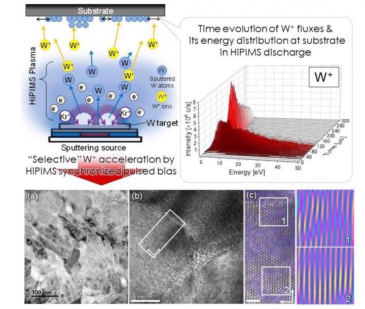
 (Top left) An illustration of the HiPIMS process. (Top right) The energy distribution of tungsten ions arriving at the substrate over time. At short times, there are a large proportion of ions with high energy. (Bottom) Stress-free tungsten films created with the selective pulsed bias technique. (a) Plan view transmission electron microscopy (TEM) image of the film; (b) a higher resolution image; (c) reconstructions of the selected area in (b) based on inverse Fourier transforms, with two regions magnified. Image Credit: Tokyo Metropolitan University.
The researchers reduced the impurities and defects to develop crystalline films with stresses as low as 0.03 GPa, similar to those realized via annealing, by improving the timing of a “substrate bias pulse” with microsecond accuracy. The research holds promise for effective pathways to make metallic films for the electronics sector.
Modern electronics is based on the intricate and nanoscale deposition of thin metallic films onto surfaces. Although this might sound easier, it is not so; if not executed properly, “film stresses” that emerge from the microscopic internal structure of the film can result in a curving and buckling over the years. Eliminating such stresses, in general, needs heating or “annealing.”
Sadly, a majority of the best metals for the job, for example, tungsten, exhibit high melting points, implying that the film must be heated to more than 1000 °C. Apart from being energy-intensive, this also severely restricts which substrate materials can be utilized. The race is on to make films with metals that have high melting points without such stresses.
A research group headed by Associate Professor Tetsuhide Shimizu of Tokyo Metropolitan University has been working on a method called high-power impulse magnetron scattering (HiPIMS), a sputtering technique.
Sputtering involves employing a high voltage throughout a metallic “target” and a substrate, thereby making plasma of charged gas atoms, which bombards the metallic target and creates a charged metal vapor. Such metal ions tend to fly toward the substrate where a film is formed.
As far as HiPIMS is concerned, the voltage is pulsed in short and strong bursts. Following each pulse, there is some separation between the arrival of metal and gas ions at the substrate — a synchronized “substrate bias” pulse can help speed up the metal ions selectively, thereby making denser films. Yet, despite several measures, the problem of residual stress continued to be the same.
At present, the researchers looked at how ions with various energies arrived at the substrate over time in unparalleled detail, with the help of tungsten and an argon gas target. Rather than making use of a bias pulse set off concurrently as the HiPIMS pulse, they utilized their know-how of when various ions arrived and added a small delay, 60 μs, to accurately choose when high energy metal ions arrive.
The researchers discovered that this helped to reduce the amount of gas that ends up in the film and effectively delivered high levels of kinetic energy. The outcome was a dense crystalline film with low film stress and large grains.
Making the bias more powerful helped the films turn out to be highly stress-free. Indeed, the effective delivery of energy to the film implied that they had achieved a similar effect to annealing when the film was deposited by them.
Additionally, swapping out argon for krypton enabled the researchers to achieve films having stress as low as 0.03 GPa, equivalent to what can be created with post-annealing.
An effective route to stress-free films will gave a considerable effect on metallization processes and also on the production of next-generation circuitry. The technology might be employed in other metals and holds the potential for huge gains for the electronics sector.
This study was financially supported by the Fund for the Promotion of Joint International Research (No.17KK0136) of the Japan Society for the Promotion of Science (JSPS), the Swedish Research Council (No. VR 2018-04139), and the Swedish Government Strategic Research Area in Materials Science on Functional Materials at Linköping University (Faculty Grant SFO-Mat-LiU No. 2009-00971).
Journal Reference:
Shimizu, T., et al. (2021) Low-temperature growth of stress-free single phase α-W films using HiPIMS with synchronized pulsed substrate bias. Journal of Applied Physics. doi.org/10.1063/5.0042608.