.jpg) By Susha Cheriyedath, M.Sc.Reviewed by Skyla BailyNov 18 2021
By Susha Cheriyedath, M.Sc.Reviewed by Skyla BailyNov 18 2021A study conducted by a team of German researchers and funded by the German federal ministry of economic affairs and energy achieved an increased certified energy conversion efficiency from 23.55% up to 24.51% for silicon heterojunction solar cells by enhancing the design of the hydrogenated intrinsic amorphous silicon on the rear side of the solar cell and the back reflector. This research has been published in the journal Progress in Photovoltaics.

Study: A route towards high-efficiency silicon heterojunction solar cells. Image Credit: Mark Agnor/Shutterstock.com
What is a Silicon Heterojunction Solar Cell?
In a silicon heterojunction solar cell (SHJ), the p-n junction is formed using silicon with two different morphologies, i.e., one is n-type crystalline silicon (c-Si), and the other one is formed by p-doped (group III element doped) amorphous silicon (a-Si). However, many researchers have reported varying the doping level, a number of layers and have added other material layers to achieve higher energy conversion efficiencies.

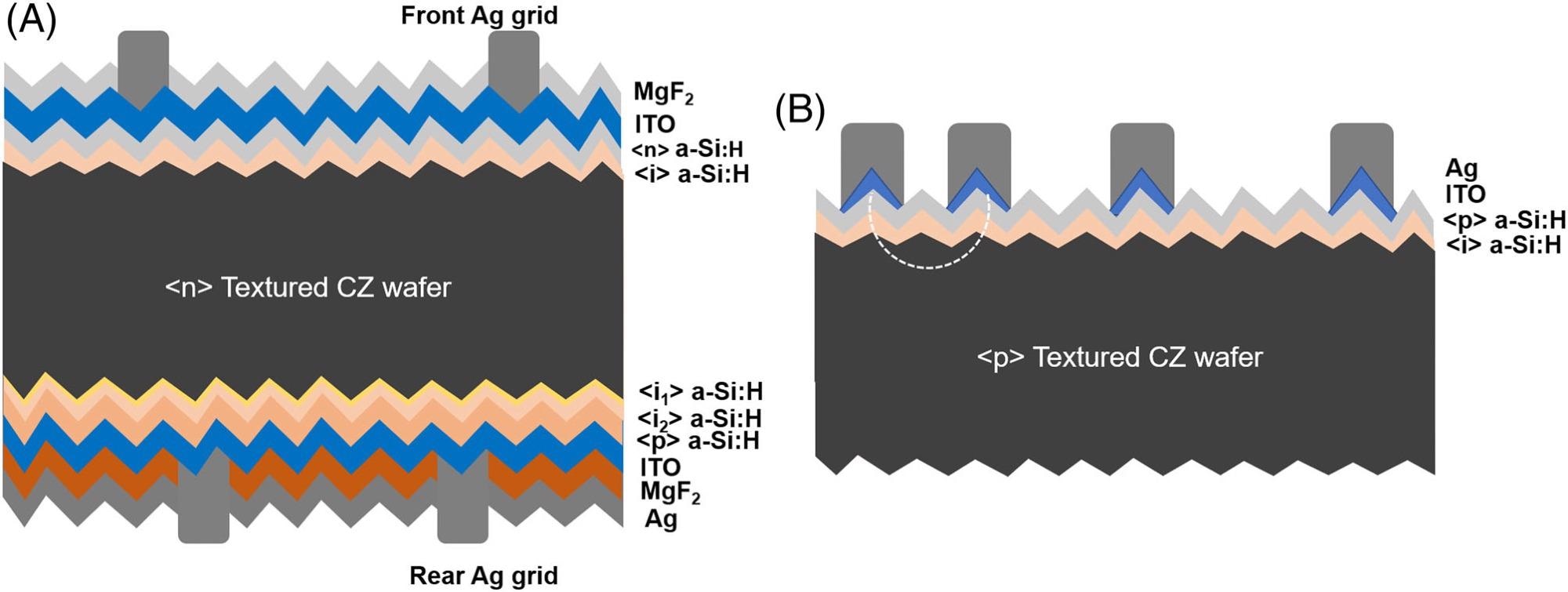
(A) Cross-sectional sketch of the certified SHJ solar cell and (B) TLM pattern structure. Image Credit: Duan W et al., Prog Photovolt Res Appl
SHJ’s high performance is driven by superior surface passivation provided by a thin hydrogenated amorphous silicon (a-Si:H) buffer layer that separates the bulk from the highly recombinative metallic contacts. As a result, very high open-circuit voltage (VOC) up to 750 mV3 is achieved.
However, the SHJ solar cells show a lower short-circuit current density and form factor compared with the other two sides contacted p- and n-type doped crystalline silicon cells due to the parasitic absorption of light at the interface of a-Si:H layers and transparent conductive oxide (TCO) layers on both sides.
What is this New Purposed SHJ Solar Cell?
The purposed SHJ solar cells are fabricated using M2-size n-type Czochralski (CZ) crystalline silicon wafers at the core. These wafers are first chemically etched to eliminate the damage and then treated in alkaline solution to obtain random pyramid textures on both sides.
Then, they are progressively cleaned in ozone, and 1% diluted hydrofluoric solution. Furthur, bi-layers of intrinsic and doped a-Si:H, respectively, are fabricated on both sides of the wafer using a plasma-enhanced chemical vapor deposition (PECVD) tool. For the second doped a-Si:H layer, the silane (SiH4)/hydrogen (H2) flow ratio and thickness are varied.
This bi-layer is crucial for enhanced efficiency. Afterward, a layer of indium-tin-oxide (ITO) is sputtered onto both sides of the wafer with a direct current mode. ITO is a transparent electron-conducting metal oxide used in many electronic display devices and solar cells.
On the top of ITO, a very thin transparent MgF2 layer is deposited, which acts as an antireflection coating layer for maximum light absorption. For the back reflector, a silver (Ag) coating was applied on the rear side.

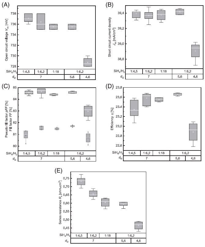
J-V parameters: (A) Jsc, (B) Voc, (C) FF/pFF, (D) ƞ, and (E) Rs of SHJ solar cells fabricated as a function of SiH4/H2 flow ratio and thickness of the i2 layer (di2). Image Credit: Duan W et al., Prog Photovolt Res Appl
What did the Study of this SHJ Solar Cell Say?
The intrinsic a-Si:H layer has multiple roles in SHJ solar cells, such as it acts as a carrier transport channel to the electrode and as a surface passivation layer. Intrinsic a-Si:H bi-layers with a porous first layer and a dense second layer are crucial to balance passivation and charge carrier transport. Both the microstructure of intrinsic a-Si:H and its thickness play important roles in solar cell performance due to the low conductivity.

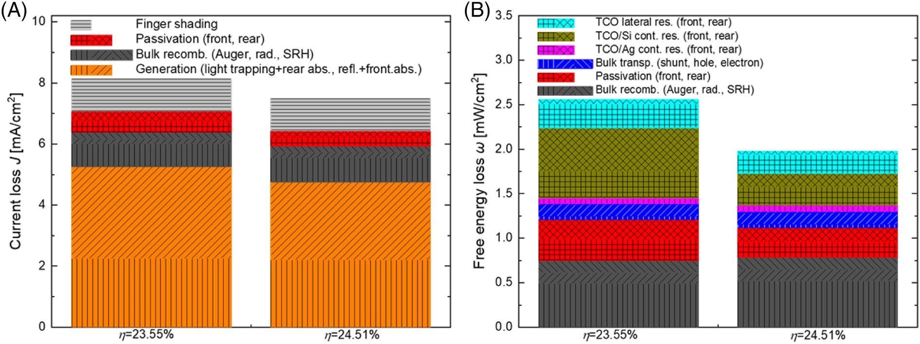
(A) Current and (B) free energy loss analysis for old and newly certified SHJ solar cells based on Quokka3 simulation. Image Credit: Duan W et al., Prog Photovolt Res Appl
In SHJ solar cells, Ag after the TCO layer acts as a back reflector and contact. However, plasmonic absorption at the rough TCO/Ag interface induced by light scattering of evanescent waves makes the effect of back reflection much less effective.
The major optical loss indicates external reflection and parasitic absorption for the previous SHJ cell, which is reduced significantly by applying the MgF2 double antireflection coating layer on the new SHJ cell.
The optical analysis suggests a further reduction in the parasitic absorption by replacing the doped a-Si:H layer with a more transparent n-type crystalline hydrogenated silicon oxide (nc-SiOx:H) layer. The research suggests that the optimization of the front TCO layer rather than using a higher quality wafer may give a slightly higher chance to increase efficiency quickly. This can be achieved by using multiple TCO layers to simultaneously meet both electrical and optical requirements.
Reference
Duan W, Lambertz A, Bittkau K, et al., A route towards high-efficiency silicon heterojunction solar cells. Prog Photovolt Res Appl. 2021;1-9. doi:10.1002/pip.3493. https://onlinelibrary.wiley.com/doi/10.1002/pip.3493
Disclaimer: The views expressed here are those of the author expressed in their private capacity and do not necessarily represent the views of AZoM.com Limited T/A AZoNetwork the owner and operator of this website. This disclaimer forms part of the Terms and conditions of use of this website.