The latest article by Chinese researchers in the journal Energy Storage Materials focuses on the advantages of silicon recycling and usage as nanowires and electrodes in lithium-ion batteries.

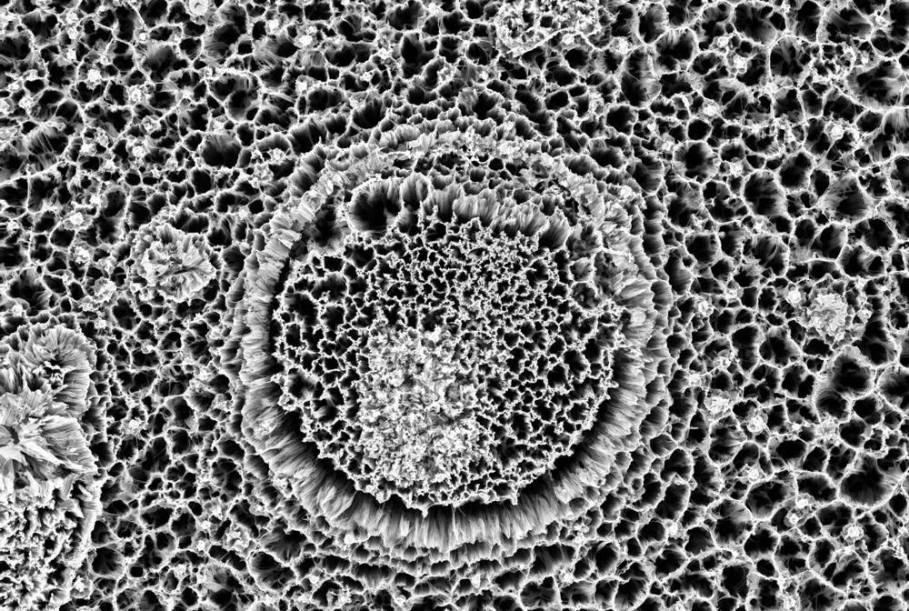
Study: Upcycling of photovoltaic silicon waste into ultrahigh areal loaded silicon nanowire electrodes through electrothermal shock. Image Credit: Roberto Lo Savio/Shutterstock.com
Silicon and Energy Storage Technology
The growth of advanced renewable energy storage systems, as well as value-added strategies for repurposing multiple sources, are critical steps toward "carbon neutrality." Clean energy production technologies such as photovoltaic systems have steadily replaced conventional fossil fuel-derived energy in recent times.
As the primary component of crystalline silicon (Si) solar cells, the global market for silicon wafers has surpassed 160 GW per year. However, during the Si wafer production process, high-purity Si that accounts for nearly 40% of the total weight of the Si ingots (purity of 99.9999%) is wasted during the wires slicing procedure, resulting in both losses of secondary source and contamination.
The Recycling Process
At the moment, the standard recycling approach based on incinerating and purification is restricted by the severe oxidation features, entrapment of residual contaminants, and high heat of vaporization of waste silicon (WSi), and can only reach reduced utilization. Furthermore, the time-consuming regeneration procedure will result in significant alternative power use and environmental re-pollution.
This is a significant violation of the original objective of ecological, affordable, and long-term growth of solar PV energy. As a result, the development of improved and clean value-added recycling technology to handle high-purity WSi will help in the PV industry's economic and environmental growth.
Silicon as Lithium-Ion Battery Electrode
The increasing usage of lithium-ion batteries (LIBs) as a driving force in the domain of high-efficiency and sustainable power storage has dramatically raised the amount of high anode material. Because of its extraordinarily high theoretically specific capacitance of 3579 mAh g1, Si is a possible next-generation high-energy-density LIB electrode material.
Upcycling PV WSi to generate high-energy-density electrode materials is predicted to accomplish a seamless connection of the Pv market with the power storage business. The micron-sized WSi particles, on the other hand, seem unable to support the stress and strain induced by the massive volumetric changes occurring during the (de)alloying operation, causing serious damage to the electrode structure.
Introduction to Silicon Nanowires
One-dimensional silicon nanowires (SiNWs) are one of the most intriguing nanostructures for use in overcoming the problems associated with Si-based electrode development.
SiNWs have several distinct benefits, including the capacity to endure severe pressure without breaking, reduced ion propagation lengths, better electron transfer, and the opportunity to expand immediately on the conductive substrate. Chemical vapor, liquid layer catalyzed development, and electrodeposition are now the most common SiNW production processes.
However, to the best knowledge, using these approaches to recreate high-purity WSi for the production of one-dimensional SiNWs is problematic. To achieve the transition of WSi into SiNWs, the stable crystalline structure of the WSi powder must be destroyed.
More from AZoM: An Overview of Polymer Upcycling
Advantages of Silicon Nanowires for Photovoltaic Applications
Silicon nanowires offer a wide spectrum of uses in semiconductors and optoelectronics. The Si nanowire-based solar cells with a radial p-n junction are one of them. Because of its outstanding optical and electrical characteristics, photovoltaic systems based on silicon nanowires (SiNWs) with a radial p-n connection have several uses.
Semiconductor nanoparticles are structures with a high aspect ratio or a high length-to-diameter ratio. This offers applications in a variety of fields. Because of their tiny size, nanowires exhibit various properties that make them appealing for photovoltaic applications. Nanowires are formed of natural silicon, have low toxicity, and are suitable with electronic circuit manufacturing technology. Furthermore, vertically oriented silicon nanowires have minimal reflection and high broadband absorption.
Research Findings
The produced SiNWs have dimensions of 50 nm, and the gaps between the nanostructures can efficiently tolerate the physical stresses generated by volume during the charging-discharging operations. The SiNWs@CC electrode with a surface loading of 4.02 mg cm2 offered the best electrocatalytic activity, according to the results.
This is mostly due to the SiNWs' inability to produce a sufficient number of current constituents when the surface load is minimal. When the surface load is too severe, the interspacing between the nanostructures narrows, and the electrical connection with the carbon fiber weakens, resulting in a drop in cycled effectiveness. Furthermore, at the half-cell level, the SiNWs@CC electrode has shown ultra-high areal strength and good long-cycle durability.
In short, the article focuses on the advantages of silicon nanowires for photovoltaic activities. The revolutionary method's effective use has therefore created a new road toward the minimal cost, large-scale production of SiNWs, and their implementation to high-energy-density power devices.
Further Reading
Lu, Jijun et.al. Upcycling of photovoltaic silicon waste into ultrahigh areal loaded silicon nanowire electrodes through electrothermal shock. 2022. Energy Storage Materials. Available at: https://www.sciencedirect.com/science/article/pii/S2405829722000587?via%3Dihub
Disclaimer: The views expressed here are those of the author expressed in their private capacity and do not necessarily represent the views of AZoM.com Limited T/A AZoNetwork the owner and operator of this website. This disclaimer forms part of the Terms and conditions of use of this website.