Reviewed by Alex SmithFeb 7 2022
Metal halide perovskites (MHPs) are defined as a class of materials exhibiting hopeful properties for semiconductor applications, like thin-film transistors (TFTs).
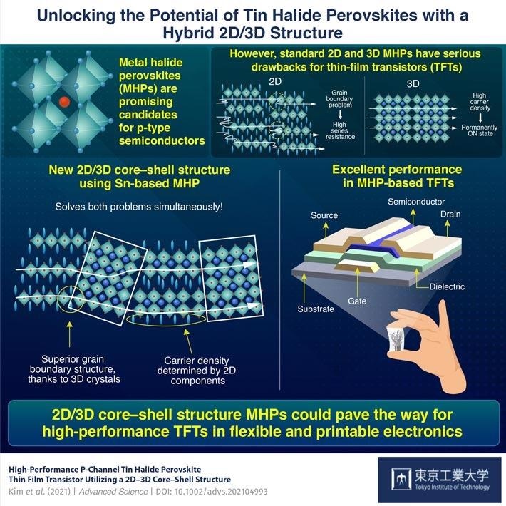 High performance P-channel Tin Halide Pervoskite Thin Film Transistor Utilizing a 2D-3D Core-Shell Structure. Image Credit: Kim, et al., 2021.
Tin (Sn)-based MHPs can be environmentally benign alternative to lead-based ones, which are deadly,but it is essential to resolve a few crucial problems before Sn-based MHPs can be introduced in planar semiconductor devices.
When organized into a 2D structure (or so-called quasi-2D structure with a few layers), defects in the crystal structure of Sn-based MHPs known as “grain boundaries” tend to hinder the mobility of charge carriers across the material.
If utilized in a TFT, this phenomenon leads to a big series resistance that eventually degrades performance. On the other hand, a TFT created utilizing an Sn-based MHP arranged into a 3D structure experiences a different yet still crippling issue.
The extremely high carrier density produced from the 3D material is responsible for forcing the transistor to be in the ON state permanently unless subjected to very high voltages. Needless to say, this makes such a device useless for several applications.
Luckily, a research group from Tokyo Tech, Japan, has discovered a solution to these restrictions. In a new study reported in the journal Advanced Science and headed by Assistant Professor Junghwan Kim and Honorary Professor Hideo Hosono, the scientists suggested a novel idea depending on a hybrid structure for Sn-based MHPs, known as the “2D/3D core–shell structure.”
In this structure, 3D MHP cores are completely separated from one another and linked only via short 2D MHP strips (or “shells”). This alternating arrangement resolves both of the abovementioned disadvantages at the same time. But how?
The trick to decreasing the series resistance of 2D MHPs is to remove the carrier mobility issues at grain boundaries. This is caused by misalignments between the conductive octahedra of the perovskite. As a result of the way in which the 3D cores link to the 2D segments, these misalignments vanish and the series resistance is significantly decreased.
As far as the high carrier density of 3D MHPs is considered, this issue is just not present when utilizing the 2D/3D core–shell structure. Because the 3D cores are detached, their carrier density is no longer appropriate; rather, the 2D segments serve as a bottleneck and restrict the effective carrier density of the entire material.
For the effectiveness of this novel structure to be illustrated, the researchers engineered a complementary metal–oxide–semiconductor (CMOS) inverter by integrated 2D or 3D TFTs with a standard indium gallium zinc oxide TFT.
Our device exhibited a high voltage gain of 200 V/V at a drain voltage of 20 V. This performance is the best reported so far for a CMOS inverter made using Sn-MHP TFTs.
Junghwan Kim, Assistant Professor, Tokyo Institute of Technology
In this study, the innovative 2D/3D structure presented will help researchers all over the world to take benefit of the appealing electronic properties of perovskites, and their method is not restricted to a narrow class of materials or device types.
The proposed strategy could be applied to various solution-derived semiconductor systems, opening doors to flexible and printable electronics.
Junghwan Kim, Assistant Professor, Tokyo Institute of Technology
Time will be the only means through which the people will get to know what technological innovations are opened by the findings of this study.
Journal Reference:
Kim, J., et al. (2021) High-Performance P-Channel Tin Halide Perovskite Thin Film Transistor Utilizing a 2D–3D Core–Shell Structure. Advanced Science. doi.org/10.1002/advs.202104993