In a recent study published in the journal Material Science in Semiconductor Processing, researchers from Egypt developed (Bi2Se3)1-x(Bi2Te3)x films with excellent optical properties.

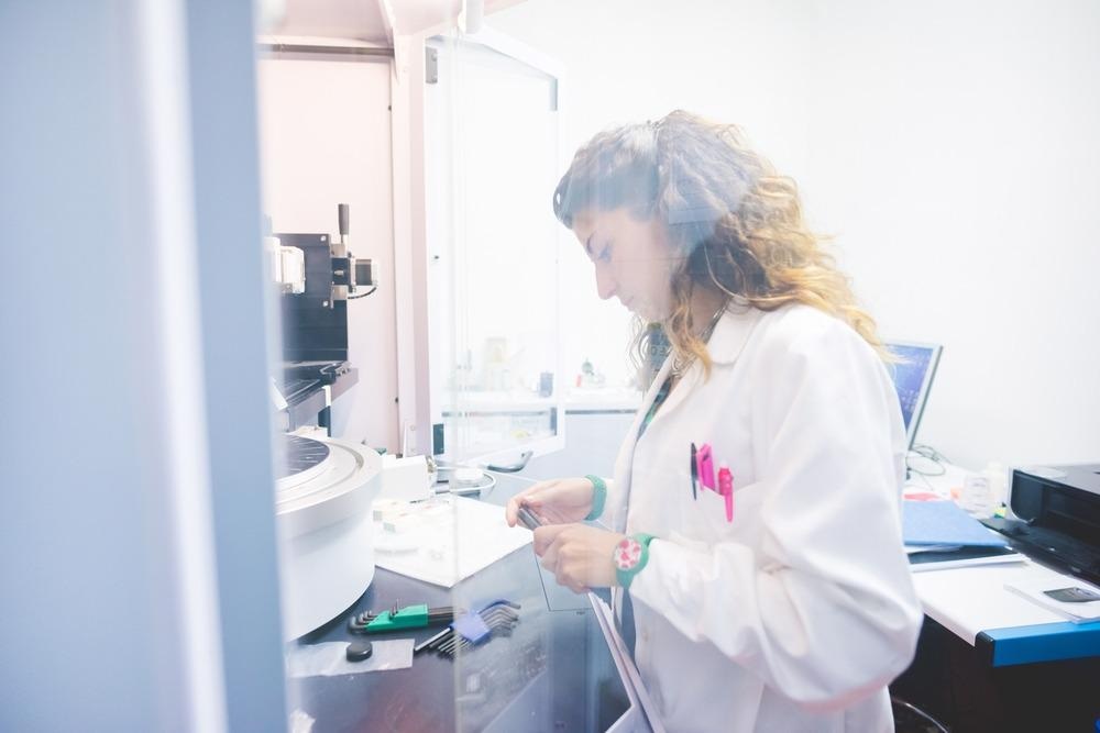
Study: Outstanding optical properties of thermally grown (Bi2Se3)1-x (Bi2Te3)x thin films. Image Credit: Image Source Trading Ltd/Shutterstock.com
Chalcogenide Materials
Chalcogenide materials consist of at least one chalcogen ion and an additional electropositive element. Chalcogenides have been used in various fields such as photo-electrochemical cells, photodetectors, and optoelectronic applications. One type of chalcogenide material is bismuth chalcogenides, which are low-band-gap semiconductors that have asymmetric band structures and rhombohedral unit cells.
Bi2Se3 is a van der Waals material having metallic surface states and other significant optical properties. In addition, Bi2Se3 has been demonstrated to be a promising material for future optoelectronic applications. Nanocrystalline layers of Bi2Se3–Bi2Te3 can also be used in information storage and quantum electronics applications.
Additionally, solar cells produced through Bi2Se3–Bi2Te3 thin film are significant for industry and research due to their low cost compared to other materials. The chalcogenides used in the present study are Bi2Te3 and Bi2Se3, which are a type of bismuth chalcogenides. Researchers alloyed the Bi2Se3 thin films with the Bi2Te3 films at different ratios and studied their optical properties.
Methodology
The materials used to develop the films were Bi, Se, and Te, with a purity of 99.99%. To develop the films, the pure element mixtures were charged into fused silica tubes that were highly evacuated and placed in a furnace for proper melting. The tubes were kept at 110°C for a time period of 12 hours for accurate melting. Further, bulk alloys were obtained after gradually cooling the furnace to room temperature.
To grow the samples, vacuum thermal evaporation was used, and the nanoparticle-based films were grown on borosilicate crown glass substrates. Initially, the substrates were thoroughly cleaned with a detergent and distilled water; ethyl alcohol and isopropyl alcohol were also used for further cleaning. The substrates were then dried using distilled water vapor.
It must be noted that the glass substrates were kept at room temperature at a fixed distance from the evaporation boat during the film's growth process. Additionally, the substrates were also rotated by a motor to get homogeneous and uniform layers of the films. Overall, six samples of (Bi2Se3)1-x(Bi2Te3)x were developed.
What Happens When the Shape of Chalcogenide Glass Changes?
The techniques used by the researchers for characterization were X-ray diffraction (XRD), scanning electron microscopy (SEM), energy dispersive X-ray (EDX) analysis, and high-resolution transmission electron microscopy (HRTEM). They also calculated the refractive index and bandgaps of the samples and plotted the variations in extinction and absorption coefficients of the films as a function of wavelength.
Results
In the XRD diffractograms of the concerned films, broad peaks were observed, which demonstrated the nano-scalability. Further, the polycrystalline nature of the grown films was confirmed by the appearance of high peaks in the XRD diffractograms.
The SEM analysis shows that the films were composed of nano-sized grains, indicating the crystalline nature of the developed films. Furthermore, the researchers observed that the surface was homogeneous and had fine and well-connected grains. The morphological properties of the film were the result of the amount of tellurium in the samples.
The HRTEM confirmed the polycrystalline nature of the samples by revealing nanocrystals that appeared as black dots. Furthermore, the selected area electron diffraction patterns confirm the crystallinity of the Bi2Se3.
The calculated bandgap of the films showed similarity with the previously published data. The widening of the bandgap of the samples was mainly due to the Burstein–Moss shift. Furthermore, the increase in the energy gap of a heavily doped semiconductor caused the shift in the band gaps.
It was observed that as the wavelength increased, the refractive index decreased. The changes in the refractive index values were due to microscopic scale imperfections in the samples. The extinction and absorption coefficient plots of the developed films showed a similarity with the non-linear behavior of the tellurium-free and tellurium-containing samples. The addition of Bi2Te3 caused an increase in both the absorption and extinction coefficients.
Conclusions
The thin (Bi2Se3)1-x(Bi2Te3)x films developed by the researchers can be used in optical recording devices. Furthermore, the results primarily indicated that the grain size decreased as the Bi2Te3 concentration increased, and films were transparent with high transparency of 81.5%.
The direct energy gap transition values ranged from 0.72 eV to 0.91 eV for all samples. It must also be noted that the addition of Bi2Te3 reduced the energy band gap and the absorption coefficient increased as the Bi2Te3 concentration increased.
Disclaimer: The views expressed here are those of the author expressed in their private capacity and do not necessarily represent the views of AZoM.com Limited T/A AZoNetwork the owner and operator of this website. This disclaimer forms part of the Terms and conditions of use of this website.
Source:
A.M. Adam, A.K. Diab, Mohamed Tolan, Z.M.H. El-Qahtani, A.A. Refaat, Medhat A. El-Hadek, E.M. Elsehly, A. El-Khouly, Abdulaziz N. Alharbi, V. Khovaylo, M. Ataalla, Outstanding optical properties of thermally grown (Bi2Se3)1-x (Bi2Te3)x thin films, Materials Science in Semiconductor Processing, Volume 143, 2022,106557, ISSN 1369-8001, https://www.sciencedirect.com/science/article/pii/S1369800122001020?via%3Dihub