Researchers have grown thin films of two diverse crystalline materials by stacking one on top of the other using a unique method referred to as “dative epitaxy.” The scientists discovered the technique inadvertently.
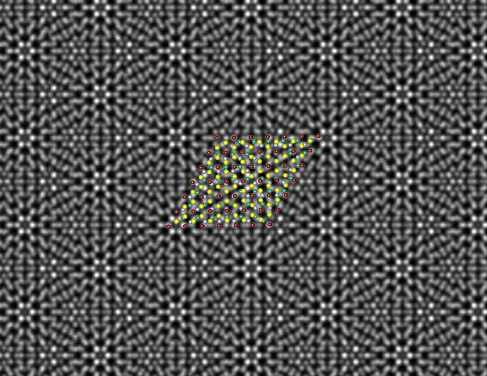
 A scanning transmission electron microscope image reveals a beautiful periodic pattern (called a “moiré pattern”) resulting from the epitaxial chromium telluride/tungsten diselenide superlattice; superimposed is the atomic model of the superlattice. Image Credit: Mengying Bian and Liang Zhu.
Hao Zeng, a physicist at the University at Buffalo (UB) explains, dative epitaxy holds together layers of various materials through a feeble attractive force between the materials, coupled with sporadic chemical bonds known as “dative bonds.”
I compare this to laying down wood floor in your home. You put a few nails in to anchor the wood planks on the surface. The dative bonds are like these nails.
Hao Zeng, Professor of Physics, College of Arts and Sciences, University at Buffalo
The study is exhilarating, Zeng states, as new methods to layer films “could have far-reaching impacts in the fields of semiconductors, quantum technology, and renewable energy.”
Zeng and his contemporaries present details about dative epitaxy in the journal Advanced Materials. The research paper was published by a collaborative team from the U.S., Singapore and China led by Zeng, Ph.D., and Mengying Bian, Ph.D., at UB; Liang Zhu, Ph.D., and Junhao Lin, Ph.D., at the Southern University of Science and Technology; and Yanglong Hou, Ph.D., at Peking University.
A ‘Fortuitous’ Discovery
“We did not start with the idea of dative epitaxy,” Zeng says. “I would say it was a fortuitous discovery. Initially, we were trying to grow atomically thin magnets on a layer of van der Waals material, which acts as a template to promote 2D growth.”
To create this magnet, Bian, a UB physics postdoctoral researcher, grew a super-thin layer of chromium telluride on the top of an extremely thin “monolayer” of tungsten diselenide.
The researchers believed the two films would be kept together just by a feeble attraction between the materials, called the van der Waals force. But viewing under the microscope exposed something surprising.
When Mengying came into the office and showed me this very nice microscope image, we immediately realized there was something unusual. The crystals looked like they were perfectly aligned with each other, and this kind of perfect alignment suggested that it might not be the van der Waals epitaxy we were expecting. In van der Waals epitaxy, the orientation of layers cannot be controlled very accurately because the layers are not strongly interacting with each other.
Hao Zeng, Professor of Physics, College of Arts and Sciences, University at Buffalo
After additional experimental and theoretical examination, in partnership with Renat Sabirianov, Ph.D., at the University of Nebraska at Omaha, the scientists decided that besides the van der Waals force, “sporadic” dative bonds linked the two films.
Next came another revelation. When Zeng hunted for current literature on dative epitaxy, he could only find one journal: a new theoretical study predicting dative bond improved van der Waals epitaxy.
The research was guided — again, unexpectedly — by his long-time associate at Rensselaer Polytechnic Institute, Shengbai Zhang, Ph.D. Zhang “was very excited to hear that our experimental discovery verified his hypothesis,” Zeng states.
“Goldilocks Principle” of Epitaxy
UB has applied for a provisional patent application for dative epitaxy approaches and is keen on expanding this investigation through a partnership with research and industry partners. Zeng and Bian say the method signifies a “Goldilocks principle” with regard to layering crystalline films.
Epitaxy requires growing a single crystalline material on top of another single crystalline substrate, with a clear orientation relationship between them. Traditional epitaxy necessitates that two materials possess comparable lattice spacing, which pertains to the distance between atoms. Van der Waals epitaxy surpasses this obstacle but can result in crystals growing in the incorrect direction.
“Dative epitaxy circumvents the stringent lattice-matching requirements in conventional epitaxy, while also taking advantage of the formation of special chemical bonds to fix crystal orientation,” Bian says.
Dative epitaxy could allow a broader range of materials to be grown. It really gives people a lot of flexibility and choice. It’s the Goldilocks principle in epitaxy: It captures the benefits of conventional and van der Waals epitaxial techniques, but addresses the drawbacks of both.
Hao Zeng, Professor of Physics, College of Arts and Sciences, University at Buffalo
Given these benefits, Zeng states, “Our technique could open the door to high-quality epitaxial growth of a variety of compound semiconductor thin films, such as, potentially, gallium arsenide or gallium nitride on silicon wafers. Integrating these materials are super important to the semiconductor industry, which has been a longstanding challenge due to the limitations of other forms of epitaxy.”
The research was chiefly financially supported by the U.S. National Science Foundation; the U.S. Department of Energy; the National Key R&D Program of China; and the National Natural Science Foundation of China. The seed funding for the study came from a grant from UB’s Vice President for Research and Economic Development.
Journal Reference:
Bian, M., et al. (2022) Dative Epitaxy of Commensurate Monocrystalline Covalent van der Waals Moiré Supercrystal. Advanced Materials. doi.org/10.1002/adma.202200117.