At Osaka University, a new technique has been illustrated by the scientists for making three-dimensional integrated circuit connections that function at low temperatures and does not need external pressure. This may result in economical and energy-efficient electronic devices.
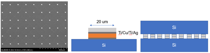 (Right) SEM image of fabricated 20-μm Cu-Ag bumps, (Middle) Schematic drawing of the prepared bump cross-section, (Left) Schematic drawing of the bonded 20-μm Cu-Ag bump device. Image Credit: Osaka University.
Researchers from the Flexible 3D-System Integration Laboratory at Osaka University came up with a new technique for the direct three-dimensional bonding of copper electrodes by making use of silver. This can decrease the cost and energy needs of new electronic devices. This work might help in the design of next-generation smart devices that utilize less electricity and are more compact.
Three-dimensional combined circuits are playing a highly significant role in electronic devices. In comparison to traditional 2D circuits, such architectures have the potential to save both spaces and decrease the material required for interconnecting wires.
But the potential to develop trustworthy 3D connections necessitates new techniques compared to the mature technologies that are used in convention integrated circuits.
Recently, a research group at Osaka University displayed how to instantly link copper electrode “bumps” with the help of silver layers.
Our process can be performed under gentle conditions, at relatively low temperatures and without added pressure, but the bonds were able to withstand over one thousand cycles of thermal shocking from −55 to 125 ºC.
Zheng Zhang, Study First Author, Osaka University
In this new technique, silver is sputtered onto the two copper surfaces to be bonded at room temperature. Heat was then employed to toughen the silver layers, thereby making the surface experience microscopic changes in a process known as “stress migration”
The liberation of the stress at the time of annealing lead to surface roughening, which guaranteed an adequately effective area between the two silver layers.
Consequently, it is possible to accomplish bonding in the absence of applied pressure even at a relatively low annealing temperature. Permanent connections that are as small as 20 µm could be identified in just 10 minutes this way. This process also only requires moderate temperatures (180 °C) and can function under atmospheric conditions.
The team was able to verify the surface roughness of the sputtered and annealed chips by making use of images by atomic force microscopy and scanning electron microscopy.
This technology is expected to contribute to chips with a high density of interconnects and advanced 3D packaging.
Katsuaki Suganuma, Study Senior Author, Osaka University