Reviewed by Alex SmithJul 26 2022
One of the most promising materials for the implementation of quantum technologies is NV-doped diamond. However, there are currently very few products available in quantities and quality that are industrially acceptable.
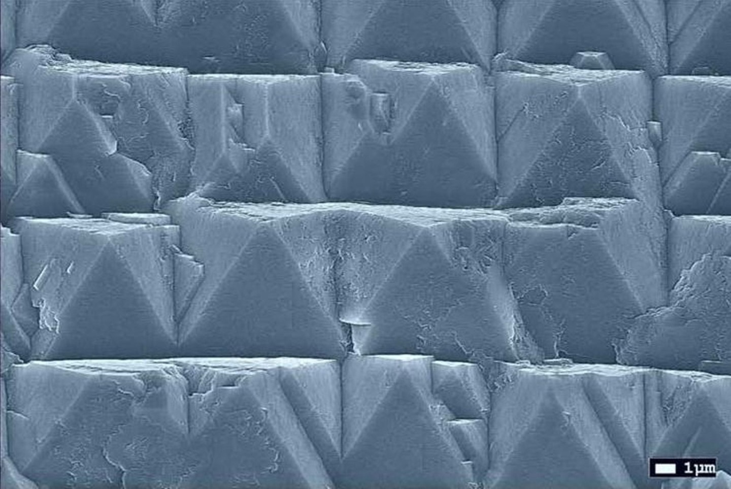
 Electron micrograph of an early growth phase of diamond on a wafer. Image Credit: Fraunhofer IAF
To facilitate the industrial application of (111)-oriented diamond substrates and the construction of a European supply chain for quantum devices, Fraunhofer IAF is working with five German firms on the BMBF-funded project GrodiaQ to create novel equipment and procedures.
The project collaboration of GrodiaQ, which stands for Large-area Diamond Substrates for Quantum Technology, has started work to secure the provision of high-purity and large-area diamond wafers for applications.
Five other firms with their own expertise in the field of production, processing, and use of diamond and diamond-based quantum technologies make up the partnership, which is supervised by the Fraunhofer Institute for Applied Solid State Physics IAF.
The project’s partners collectively span the whole value chain. The goal is to create production tools and raw materials for quantum devices that the industry partners can use commercially after the project is complete. The initiative will be supported for three years by the German Federal Ministry of Education and Research (BMBF).
Large-area high-quality diamond wafers are an irreplaceable basic component in the production of devices for diamond-based quantum technologies, which are expected to reach the market in the next three to ten years.
Dr. Peter Knittel, Project Coordinator, Fraunhofer IAF
Dr. Knittel added, “Material costs can be significantly reduced by using diamond wafers with larger diameters compared to the current state of the art, making the development and production of quantum devices economical. Against this background, GrodiaQ is a great opportunity to establish Germany as a leading location in the research, development and production of advanced diamond-based quantum technologies.”
(111)-Oriented Diamond Substrates in Sizes Suitable for Industrial Use
Diamond’s nitrogen-vacancy centers (NV centers) can create stable quantum states at ambient temperature, thanks to certain material features.
Due to this, one of the most promising methods for applying and commercializing quantum technologies, such as in the fields of computer science (quantum computing) and medical technology (quantum sensing), is the usage of NV centers in diamond substrates.
Diamond grown in the (111)-oriented crystal direction is a crucial material for the production of quantum devices since this growth enhances the development of NV centers by making nitrogen incorporation easier and also greatly increases their controllability as qubits.
However, it is still difficult to find a diamond substrate that meets the aforementioned requirements. Few producers, not including anyone from the European Union (EU), are capable of producing any material that satisfies the required criteria for crystal clarity and (111) orientation.
Additionally, availability is restricted to non-industrial small quantities and the usual 3×3 mm size.
Another difficulty is the brittleness of the available substrates, which must be refined to a surface roughness of under 2 nm for use in quantum technologies.
In contrast, the diamond wafers designed for GrodiaQ have a size that is acceptable for industrial use and, at the same time, are the optimum substrates for subsequent preparation and processing due to the improved processing methods.
European Supply Chain for Sovereign Material Supply
The GrodiaQ project partners intend to allow industrially applicable diamond substrates in three phases and thereby build the groundwork for a European quantum device supply chain. Fraunhofer IAF offers resources, expertise, and infrastructure for the duration of the project, in addition to project coordination.
Additionally, it focuses on enhancing the heteroepitaxial development of (111)-oriented diamond to create functional layers for applications in quantum technology.
Diamond Materials, in close collaboration with Fraunhofer IAF, is in charge of growing and processing bigger substrate areas and volumes, as well as grinding and polishing to the roughness of less than 2 nm.
By utilizing new semiconductor microwave generators from TRUMPF Hüttinger in conjunction with an energy-efficient chemical vapor deposition (CVD) reactor based on the bias-enhanced nucleation (BEN) method, Evatec Europe hopes to meet industry requirements for wafer coating starting at 4 inches.
The BEN reactor’s chamber geometry and voltage distribution have a significant impact on the quality of the diamond coatings, and the generators’ ability to produce a uniform microwave plasma across a greater region has an impact on the homogeneity of the plasma.
In addition, the affiliated partners, Q.ANT and Quantum Brilliance, will assess the substrates described at Fraunhofer IAF in terms of their potential applications in the areas of quantum sensing and quantum computing and will release them to the market following the project.