Physical failure analysis has become more challenging especially on accounts of continuous dimensional scaling of CMOS. In order to fulfill the sophisticated circuit designs and functions, it is imperative to increase the number of transistors and layer stacks. Hence, layer-by-layer deprocessing is becoming increasingly crucial, challenging and time consuming for multiple industrial and research applications such as physical failure analysis, reverse engineering of the chips, and patent violation checks.
Delayering consists of strategically removing a set of layers to isolate a structure of interest. It is a key sample preparation technique in today’s semiconductor industry especially for technology chips of sub-20 nm nature. Up until recently, IC delayering was implemented by using chemical etching, or by mechanical polishing to the desired layer of interest. While these techniques offer a solution for fast chip deprocessing, their main drawback lies in the lack of localized and precise layer removal capability. Indeed, stopping at a desired layer is difficult, and it becomes really challenging if not impossible, for today’s sub-20 nm node technologies. On the other hand, chemical agents used for delayering can be very aggressive to the chip components and, in some cases, lead to their complete destruction.
Gallium FIB combined with dedicated gas chemistry can remove the dissimilar materials with almost the same material removal rates allowing final RMS of planarity of layer exposed to under 10 nm topography overall. Standard ion beam sputtering from a gallium FIB with its many benefits often requires the incorporation of special precursors that can help make the milling operations smoother by mitigating the side effects of re-deposition, and help overcome or achieve selective etching. While gallium ion implantation induces changes in the electrical characteristics of the prepared samples, this is not suitable for electrical nanoprobing (Xe plasma FIB used in delayering applications for the purposes of electrical testing with nanoprobes). However, delayering on semiconductor chips can still be performed for applications such as reverse engineering, cyber-security and physical failure analysis workflows for eventual lamella preparation since in these applications the interest is more focused on studying the unique architectural or material characteristics information. It is extremely effective in terms of initial planar removal of multiple layers and then performing TEM lamella preparation in areas of interest.

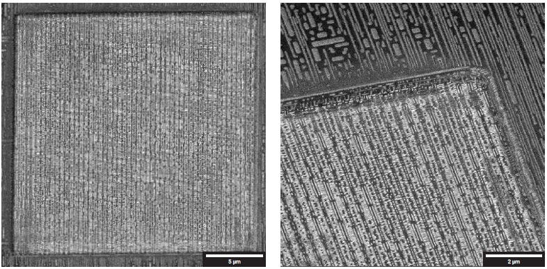
Figure 1: (Left) Overview of delayered area (20 × 20 μm2) down to via contact layer. (Right) Detail showing smooth polished walls.
Procedure Details and Results
The point of critical interest for gallium FIB-based delayering is the same as with Xe plasma FIB – the ability to stop the process accurately at any chosen depth in thin sensitive layers of metal or via. This is done so that the planarity of the substrate remains true to its original design. This helps identify faulty design and irregularities in logic circuitry in any given layer that can somehow alter or manipulate its intended functionality.
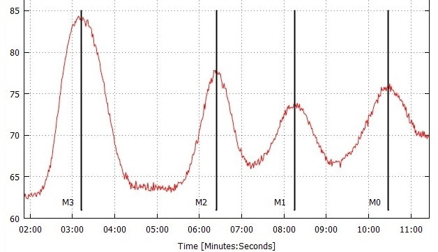
In this application note, we present front-side delayering performed on an Exynos 10 nm node process chip using the new TESCAN S9000G Ga FIB-SEM system. The top layers of the die were removed using mechanical polishing, exposing a gradient with accessibility to deep underlying layers. Fig. 1 (left) shows the via contact layer delayered over an area of 20 × 20 μm² using our proprietary gas chemistry in the presence of low beam current and relatively lower beam energies. The dissimilar material is observed to have been removed in a planar fashion, see Fig. 1 (right). The method provides significant advantages in terms of localized, precise and layer-by-layer removal possibility with constant monitoring using the end-point detection with acquired SE signal – the SE signal when collected and plotted acts as a control parameter where each peak represents a metal line while every trough represents a via layer (Fig. 2).

Figure 2: End-Point Detection (EPD) curve for monitoring and controlling the delayering process – which in this example stopped at the transistor contact layer.
The architectural study of the microprocessor chips often taken over by independent service labs, will find this application of vital importance especially for recognizing the malicious logic gate alterations that can somehow be used in spy operations. It can help uncover patent violation or faulty design information. Today, gallium FIB has become more important than in the earlier industrial era and will likely continue to play an advancing role in semiconductor technological growth.
Conclusions
In this application example, we have shown that the delayering process implemented with the new TESCAN S9000G FIB-SEM in combination with proprietary gas chemistry, is capable of performing delayering for 10-12 layers on sub-20 nm process nodes and more. It enhances the workflow capability by being able to perform ultra-thin lamellae post-delayering for TEM-based analysis making the TESCAN S9000G a ‘must-have’ tool in semiconductor physical failure analysis.
TESCAN Group
Founded in 1991 by a group of managers and engineers from Tesla with its electron microscopy history starting in the 1950’s, today TESCAN is a globally renowned supplier of Focused Ion Beam workstations, Scanning Electron Microscopes and Optical Microscopes. TESCAN’s innovative solutions and collaborative nature with its customers have won it a leading position in the world of nano- and microtechnology.
In 2019, TESCAN launched their new Generation IV series of SEMs and FIB-SEMs to the global marketplace. These state-of-the-art systems provide the most advanced capabilities and quality performance for sample preparation.
TESCAN Group is the North American arm of TESCAN Group, a multinational company established by the merger of Czech company TESCAN, a leading global supplier of SEMs and Focused Ion Beam workstations, and French company ORSAY PHYSICS, a world leader in customized Focused Ion Beam and Electron Beam technology.

This information has been sourced, reviewed and adapted from materials provided by TESCAN Group.
For more information on this source, please visit TESCAN Group.