An automated version of the PI 89 system created for high-throughput testing is called the PI 89 Auto. By using encoded linear stages, a dual-configuration rotation and tilt (R/T) mechanism, and a seamless imaging/Electron Backscatter Diffraction/Energy Dispersive Spectroscopy (EBSD/EDS) interface, it can do these tasks simultaneously.
PI 89 Auto Includes
- Base PI 89 platform with controller
- Advanced rotation and tilt (R/T) stage
- TriboScan Auto software, which allows automated testing
The main objective of PI 89 Auto is to establish a connection between the composition, processing, and properties of various materials. Understanding the connection between a material's microstructure and its mechanical and functional properties can be aided by this connection. With the ability to enhance industrial processes and the performance of materials used in various sectors, PI 89 Auto presents an innovative achievement in materials testing and analysis.

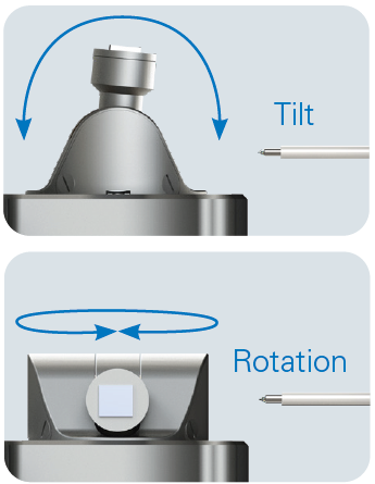
Figure 1. The SEM and EDS signals can be captured by using the tilt function of the R/T stage, and EBSD mapping can be obtained using the rotation and tilt functions. Image Credit: Bruker Nano Surfaces and Metrology
PI 89 Auto Delivers
- Automated nanoindentation with low operator interaction and high throughput
- Using SEM imaging and EBSD/EDS analysis, co-localized metrology is used to promote the development of new materials by correlating structure, processing, and property
- Patented dual-configuration rotation and tilt stage that enables simple alignment with the correct detectors
Case Study: Laser Clad Region
The PI 89 Auto was used to study the laser-clad area of 410 stainless steel on a 4140 steel substrate. During the laser cladding process, a heat-affected zone (HAZ) is formed at the base of the laser cladding region.
SEM imaging
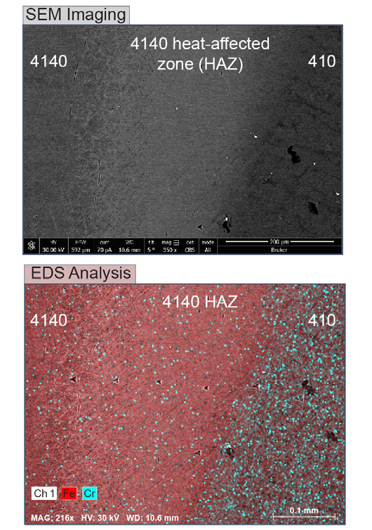
Three distinct layers were discovered: the 4140 substrate, the HAZ of the 4140 substrate, and the 410 stainless steel.
EDS elemental analysis
The 410 stainless steel area had chromium-rich layers, whereas the 4140 substrate and HAZ had iron-rich phases.
Nanoindentation for mechanical properties
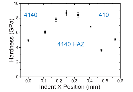
The TriboScan Auto software was used to pick out seven positions across the layers on the live SEM image. Partially unloaded indentations were performed at these locations, and hardness and modulus profiles were created.
Correlated results and analysis
According to the results, the heat-affected zone had a higher hardness than the 410 stainless steel and the 4140 substrate. The high heat changes the microstructure of 4140 steel, increasing hardness from a thin layer with tiny grains and martensite at the grain boundaries.


Figure 2. Co-localized SEM imaging (top), EDS analysis (middle), and hardness profiling (bottom) of a laser clad region of 410 stainless steel onto a 4140 steel substrate. Image Credit: Bruker Nano Surfaces and Metrology
PI 89 Auto Specifications. Source: Bruker Nano Surfaces and Metrology
| . |
. |
| Load with base PI 89 Auto |
10 mN |
| Load noise floor |
<400 nN |
| Maximum displacement with base PI 89 Auto |
5 μm |
| Displacement noise floor |
<1 nm |
| Option – Maximum load |
300 mN |
| Load noise floor |
<5 μm |
| Option – Maximum displacement |
150 μm |
| Displacement noise floor |
<1 nm |
| Stage travel (x, y, z), where y is the indentation axis |
26 mm, 29 mm, and 12 mm |
| Linear stage resolution |
1 nm |
| R/T stage travel |
180° and 90° |
| R/T stage resolution |
0.33° rotation stage, 0.18° tilt stage |
| Overall positioning accuracy from imaging and EBSD position |
Typically 5 μm* |
*The accuracy specification may change depending upon the SEM environment, SEM stage encoder, stage heating, and drift. Guaranteed accuracy <30 μm.