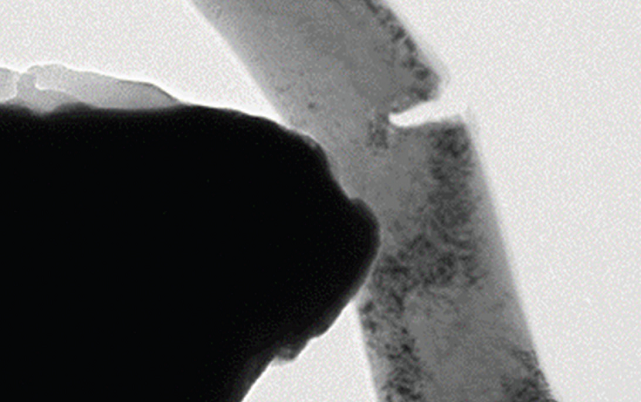
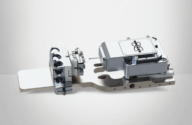
With the Hysitron PI Series PicoIndenters, Bruker makes it simple to conduct in-situ mechanical studies in the scanning electron microscope (SEM) or transmission electron microscope (TEM). Users are guaranteed to discover an ideal solution for their study with options built to match most microscope brands.

Image Credit: Bruker Nano Surfaces and Metrology
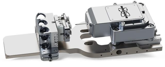
Hysitron PI 89 SEM PicoIndenter
Advanced versatility for testing in extreme environments
- Absolute quantitative nanoscale mechanical characterization by direct observation, with up to 3.5 N load and 150 µm displacement
- Encoded XYZ sample location, a strong mechanical design, a flexible platform, and a lighter weight
- The comprehensive array of testing methodologies, including 1000 °C heating, cryogenic temperature, scratch, electrical characterization, scanning probe microscopy (SPM) imaging, XPM property mapping, fatigue/nanoDynamic, and more, are supported by a modular design

Image Credit: Bruker Nano Surfaces and Metrology
The PI 89 allows researchers to conduct in-situ nanomechanical testing inside an SEM from extremely low to high loads while providing exceptional environmental control. The system combines Bruker’s high-performance controller with a proprietary capacitive transducer and intrinsic displacement control flexure technology. This results in industry-leading force and displacement resolutions and increased force and displacement ranges.
The modular architecture also enables various testing methodologies for future upgrades, such as heating and scratch testing.

Image Credit: Bruker Nano Surfaces and Metrology
SEM PicoIndenter Specifications. Source: Bruker Nano Surfaces and Metrology
| Feature |
Hysitron PI 85E |
Hysitron PI 89 / PI 89 Auto |
| Max Force |
10 mN; 250 mN |
10 mN; 500 mN; >3.5 N (300 mN max load for PI 89 Auto) |
| Force Noise Floor* (inside an SEM, 60 Hz) |
<0.4 μN; <5 μN |
<0.4 μN; <5 μN; 30 μN |
| Force Noise Floor (in ideal environment, 60 Hz, 10 mN transducer) |
<50 nN |
<50 nN |
| Max Displacement |
5 μm; 100 μm |
5 μm; 150 μm |
| Displacement Noise Floor* (inside an SEM, 60 Hz) |
<1 nm |
<1 nm |
| Displacement Noise Floor (in ideal environment, 60 Hz, 10 mN transducer) |
<0.1 nm |
<0.1 nm |
| Feedback Control Rate |
78 kHz |
78 kHz |
| Max Data Acquisition Rate |
39 kHz |
39 kHz |
| Sample Positioning Range |
>3 x 3 mm (XY, in sample plane); 20 mm (Z, manual) |
12 x 26 mm (XY); 29 mm (Z) |
*Guaranteed on install.