Jul 31 2008
Hitachi Ltd and Hokkaido University prototyped an electron analysis microscope that produces an enlarged image by irradiating an electron beam from a scanning electron microscope (SEM) to a specimen and analyzing the diffraction pattern of the scattered light.
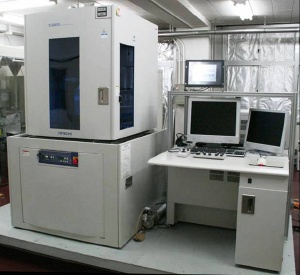
 The appearance of the prototyped equipment. An existing SEM was modified to build the prototype.
Because the output of the electron beam is as low as 30keV, light element materials such as carbon can be observed without damage to the specimen. Unlike existing microscopes, distortion from aberration is limited in the prototype, because it does not use imaging lens.
"The actual prototype of an analysis microscope without an imaging lens is the first in the world," said professor Kazutoshi Gohara of Hokkaido University Graduate School of Engineering. The nanotube specimen was observed at 0.34nm resolution, according to Gohara.
In general, a transmission electron microscope (TEM), in which parallel electron beams of approximately 100keV irradiate a specimen, is used for electron level observation. However in this method, because of the high energy, damages such as displacement of atoms could occur in the specimens, making long-time or repeated observation difficult. In addition, distortion and blur due to aberration of lens are likely to occur, because images are enlarged by a imaging lens.
Hitachi and Hokkaido University solved these problems by applying the principle of an analysis microscope on an SEM, in which the output of the electron beam is small. The low-output equipment is of about the same size as an SEM, while its resolution is expected to be equivalent to that of a TEM.
The prototype built by Hitachi and Hokkaido University is a modification of an SEM. The modification was made on the irradiation optic system of an existing SEM to irradiate beams with high parallelism so as to obtain a diffraction pattern. A camera chamber adopted by a TEM, which is equipped with a film driving mechanism and a shutter, was also added to record diffraction patterns.
In addition, Hokkaido University developed an algorithm for data processing software and built an exclusive cluster system, because thousands to ten thousands of Fourier transformations and inverse Fourier transformations are required to obtain observation images from diffraction patterns, according to a source.
This research has been adopted by the Japan Science and Technology Agency as a research theme and further efforts will be made for energy reduction as well as improvement of resolution, according to Osamu Kamimura, senior researcher at the Advanced Technology Research Department in the Central Research Laboratory of Hitachi Ltd. However, he did not disclose a timeframe for commercialization.
For commercialization, some improvements are needed, including reduction of noise signals caused by inelastic scattering that attenuates the power of irradiation beams and disturbance from the equipment as well as parallelism of electron beams, according to Kamimura.
In a diffraction microscope, electron beams irradiate a specimen, through which a diffraction pattern image data is obtained, and an enlarged image of the specimen is obtained through an arithmetic processing of the data by a computer.
The principle was suggested in the 1950s and researches toward the realization started in early 1070s. Proving tests in laboratories have been carried out since early 1990s. X-rays and laser beams are used in some researches, but they are inferior in resolution capacity because the wave length is longer than that of leaser beams.
For more information on electron microscopes , click here.