Mar 17 2009
Researchers at Rensselaer Polytechnic Institute have developed a new technique for growing slimmer copper nanorods, a key step for advancing integrated 3-D chip technology.
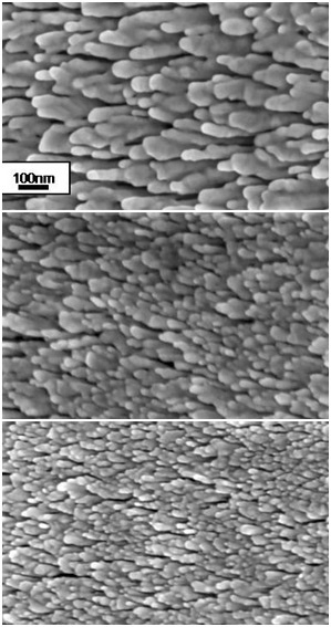
 Researchers at Rensselaer Polytechnic Institute have discovered a new method for growing slimmer copper nanorods, which can be used as a low-temperature bonding agent for holding together the layers of next-generation 3-D integrated computer chips. The researchers found that interrupting the nanorod growth process results in thinner rods. Pictured are scanning electron images, at the same magnification, of copper nanorods that have been grown without interruption (top), with two interruptions (middle), and with six interruptions (bottom).
These thinner copper nanorods fuse together, or anneal, at about 300 degrees Celsius. This relatively low annealing temperature could make the nanorods ideal for use in heat-sensitive nanoelectronics, particularly for “gluing” together the stacked components of 3-D computer chips.
“When fabricating and assembling 3-D chips, and when bonding the silicon wafers together, you want as low a temperature as possible,” said Pei-I Wang, research associate at Rensselaer’s Center for Integrated Electronics. “Slimmer nanorods, by virtue of their smaller diameters, require less heat to anneal. These lower temperatures won’t damage or degrade the delicate semiconductors. The end result is a less expensive, more reliable device.”
Experimental 3-D computer chips are comprised of several layers of stacked components. Wang said these layers can be coated with thin nanorods, and then heated up to 300 degrees Celsius. Around that temperature, the thin nanorods anneal, turn into a continuous thin film, and fuse the layers together. This study was the first demonstration of slimmer nanorods enabling wafer bonding, according to Wang.
Fundamental research concerning the slimmer nanorods was led by Toh-Ming Lu, the R.P. Baker Distinguished Professor of Physics at Rensselaer. Results of the study were recently published in the journal Nanotechnology.
Research into wafer bonding and incorporating the slimmer nanorods into 3-D integrated computer chips was led by James Jian-Qiang Lu, associate professor in the Department of Electrical, Computer, and Systems Engineering (ECSE) and the Center for Integrated Electronics (CIE) at Rensselaer. Results of the study were recently published in the journal Electrochemical and Solid-State Letters.
The slimmer copper nanorods were formed by periodically interrupting the growth process. The vapor-deposition process was occasionally halted, and the fledgling nanorods were exposed to oxygen. This resulted in a forest of nanorods with diameters between 10 nanometers and 50 nanometers – far smaller than the typical 100-nanometer diameter copper nanorods grown conventionally without interruption.
Vast forests, or arrays, of copper nanorods are produced by vapor deposition at an oblique angle. In a conventional setting, with an uninterrupted stream of copper atoms deposited in a vacuum onto a substrate, the deposition angle naturally results in taller, thicker nanorods.
Periodically interrupting the deposition, and exposing the copper nanorods to ambient air, however, leads to oxygen being absorbed into the surface of the nanorods. During subsequent depositions, this oxidized copper helps to prevent the vaporized copper atoms from migrating away from the very tips of the nanorods. This ensures the nanorods grow taller, without necessarily growing in diameter. The more growth interruptions, the thinner the resulting nanorods, Wang said.
Wang and the research group have filed for a patent for this new technology. The patent is currently pending.
Along with Wang and Toh-Ming Lu, co-authors of the Nanotechnology paper include Gwo Ching Wang, professor and chair of the Department of Physics, Applied Physics, and Astronomy at Rensselaer; Rensselaer physics graduate student Thomas C. Parker; and Tansel Karabacak, assistant professor in the Department of Applied Science at the University of Arkansas at Little Rock.
Co-authors of the Electrochemical and Solid-State Letters paper include Pei-I Wang, Toh-Ming Lu, James Jian-Qiang Lu, Parker, Karabacak, along with Rensselaer research associate Sang Hwui Lee, and Rensselaer Center for Integrated Electronics Senior Applications Engineer Michael D. Frey.
Funding for the research reported in the Electrochemical and Solid-State Letters was provided by the New York State Foundation for Science, Technology and Innovation (NYSTAR) through the Interconnect Focus Center-New York.
Visit Toh-Ming Lu’s Web site for more information on advanced thin-film research, or James Jian-Qiang Lu’s Web site for more information on research into 3-D integrated semiconductors.