Sep 16 2009
A doctoral student at the research center Forschungszentrum Dresden-Rossendorf (FZD) suggests interpreting the images generated by Kelvin probe force microscopy in a new way. She recently published her insights in the journal „Physical Review B“.
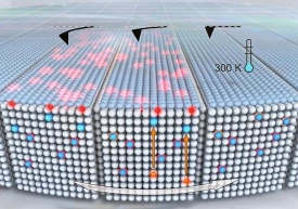
 Schematic drawing of a Kelvin probe force microscopy probe above a doped semiconductor with a thin oxide layer (grey blue atomic layer). Occupied surface states at the interface between the oxide layer and the semiconductor are animated in red and the same number of unscreened dopant atoms is animated in dark blue. The resulting asymmetric electric dipole causes the deflection of the probe (left). By applying a bias mobile majority charge carriers are injected into the semiconductor (animated in orange) and screen the unscreened ionized dopant atoms (center). As a result the electrostatic force onto the cantilever vanishes. The cantilever moves back to its normal position (right). The applied bias is measured and depends on the concentration of dopant atoms.
The last years have seen a tremendous progress in microscopic technologies. Modern microscopes are able to three-dimensionally map molecules, to identify smallest structures like single atoms, or even to distinguish between different sorts of atoms. Atomic force microscopy is well-known even in the public as a versatile tool for the production of images on the nanoscale level. Kelvin probe force microscopy is a special type of this imaging technique named after Lord Kelvin. When brought to the market in 1991, a scientific description of how to interprete the images was delivered. To this, physicist Christine Baumgart, a doctoral student of the nanospintronics group at the FZD, has now added new features.
Atomic force microscopes come along with a resolution even beyond the nanoscale level (the gap between two atoms averages 0.2 nanometers). Such a microscope generates an image of the surface topography by moving a tiny tip fixed on a small beam (cantilever) over the sample under investigation. The tip interacts with the atoms sitting on the surface of the sample, allowing the atoms to exert a force on the tip. This force affects the cantilever as well, whose deformation can be measured by a laser system. A Kelvin probe force microscope uses an electrically conducting tip. Therefore it measures not only the surface topography of the sample, but also the electric force between the tip and the sample. Hence surface phenomena like catalytic or electric activity of ion doped materials can thoroughly be investigated. While this microscopic technique is advantageous for non-destructive investigation of electric properties, the complicated measuring procedure, which even affects the reproducibility of the scientific outcome, is considered to be its main disadvantage. Furthermore, scientists have relied on an incomplete explanation for the values they measured because it has been believed that the electric potential between the tip and the surface of the sample was measured.
Christine Baumgart now discovered what exactly is measured by Kelvin probe force microscopy. It is the electric potential which is needed to move electrons or holes from the inside to the surface of a semiconductor. Her new findings will simplify the microscopic technique itself, and will lead to unambiguous and reproducible results concerning the structure and electronic properties of samples. Also, Kelvin probe force microscopy, which has been used mainly in materials science and semiconductor physics so far, is likely to become more attractive for other areas like biotechnology.
But how exactly does a Kelvin probe force microscope work? The tip is deflected by the electrostatic force between cantilever and sample when moved over the sample. By applying bias to the sample, electrons and holes are moved to the surface of the semiconductor and the electrostatic force decreases. The cantilever moves back to its original position and the applied bias is stored as the signal measured. To be more precise, there is a quantitative relation between the measured Kelvin bias and the difference between the calculated Fermi energy and respective semiconductor band edge independent of the work function of the probing microscope tip. Thus, Christine Baumgart’s novel explanation of how the Kelvin probe force microscope works elucidates why the signal depends on the bias necessary for injecting majority charge carriers towards the interface between insulator and semiconductor.
In her dissertation work under the supervision of Dr. Heidemarie Schmidt, Christine Baumgart deals with materials for future nanospintronic devices. Usually, foreign atoms are implanted into these materials. To describe doped semiconductors thoroughly, she uses various microscopic techniques like the Kelvin probe force microscope. Christine Baumgart: “I wanted to understand more precisely how this microscope works. At the Ion Beam Center of the FZD we are able to produce especially well defined samples. While working with such semiconducting samples, I found out what exactly the Kelvin probe force microscope measures and that the signal has not been interpreted sufficiently. The good news is that the measurement itself has always been correct.”