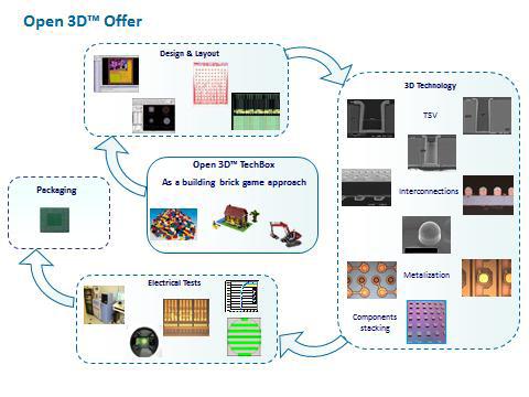
CEA-Leti has released a new platform for offering mature three dimensional pioneering technologies to the academic and industrial partners for their research projects and advanced products.
 Open 3D Platform
The new Open 3D platform from Leti has included layout, 3D design and technologies that incorporate assembly of TSV and components, interconnections, final packaging and reliability tests for systems achievement. This platform helps the company’s partners to solve challenges in main technologies.
Proven “off-the-shelf” 3D technologies of Leti has been integrated in the Open 3D platform and offer significant benefits in cost, form factor and performance for several markets such as space and aerospace, medical or bio, security and defense, consumer applications, or primary research.
The customers are enabled by this 3D platform to reach a proof of concept using small amount of wafers or prototyping with huge amount. The offer depends on limited mature technologies to assure performances, moderate costs, and short cycle times according to Leti clients’ primary technical needs.
Open 3D platform directly functions on passive wafers for interposer technologies and on active wafers, along with embedded parts. This platform works on the Minatec Campus in Grenoble through technological platforms and Leti teams.
This Open 3D platform is functioning for 200 mm wafers and will be working for 300 mm wafers in 2012.
Under-bump metallurgy (UBM), through silicon vias (TSV), redistribution layers (RDL), bumps technology-based interconnects for chips to substrates, micro-bumps technology-based interconnects for chips to wafers, debonding, thinning and temporary bonding are the modules included in the technology catalogue of the platform.