May 6 2014
An enormous treasure slumbers in the depths of our planet. Temperatures of up to 7000 °Celsius are thought to be present in the Earth's core, while at a depth of four to six kilometers (2.5 to 3.5 miles) it is still 150 °C to over 200 °C. These gigantic reserves of heat can be used as a renewable source of energy for geothermal power.
The drill bits and bore hole probes employed are high-tech machines. They are fitted with a range of sensors and control mechanisms for their expedition into the Earth's interior. They are able in this way to be very precisely controlled or autonomously analyze the environmental parameters at depth, and thereby locate suitable – in other words, warm – regions for geothermal production. There is one problem, however: microchips hit their thermal limits when exposed to temperatures over 200 degrees Celsius.
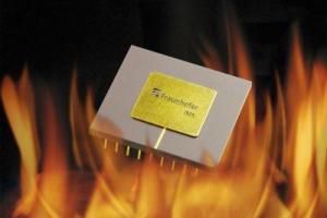
 Keeping their cool at 300 °C are: the especially compact microchips of Fraunhofer IMS. Credit: © Fraunhofer IMS
Withstanding temperatures of several hundred degrees Celsius
Scientists of the Fraunhofer Institute for Microelectronic Circuits and Systems IMS have now developed a new type of high-temperature process. "It becomes possible with this process to fabricate extremely compact microchips that operate flawlessly even at temperatures of up to 300 degrees Celsius," according to Holger Kappert, head of High-Temperature Electronics at Fraunhofer IMS. It is true that conventional semiconductor chips (CMOS) sometimes tolerate temperatures of up to 250 degrees Celsius, but their performance and reliability fall off rapidly. Frequently, companies must test a large quantity of standard chips using the trial-and-error method before they obtain an acceptable selection – a laborious undertaking.
An additional avenue exists – continuously cooling the heat-sensitive microelectronics, which can hardly be accomplished without extensive additional effort being necessary, however. There are also specialized high-temperature chips on the market already – but with about one micrometer minimal structure size, they are very large. "The solutions available are always associated with certain trade-offs: either they have comparatively large components, or they function with limited performance," Kappert summarizes.
The microchips from IMS are different, though. At a characteristic dimension of 0.35 µm, they are considerably smaller than the high-temperature chips available today. The advantage of these kinds of complex microstructures can be summarized as "more functionality at less size". That is what is necessary to make the chips more capable and more inteligent as well. To fabricate the heat-tolerant mini-chips, the researchers in Duisburg, Germany, use a specialized high-temperature SOI CMOS process. "SOI stands for 'silicon-on-insulator' – that means we introduce a layer that insulates the transistors from one another," explains Kappert. This insulation prevents leakage currents that occur from influencing the operation of the chip. Leakage currents are electrical currents flowing over other than intended paths. They are caused or increased by elevated temperatures in particular. Moreover, the researchers use tungsten metallization for their chips, which is less temperature sensitive than the aluminum usually used. This increases the operating life of the high-temperature chips.
Environmentally friendlier flight
Production of geothermal energy, natural gas, or oil is not the sole area of potential application. The microchips could also prove valuable to aviation, for instance by enabling sensors to be located as close as possible to turbine engines in order to be able to observe the state of their operation. This could permit the turbines to be operated more reliably and efficiently, saving jet fuel and thereby making aviation environmentally friendlier. The first field tests of the new chips have been positive. The researchers want to offer the fabrication process as a service later this year.