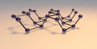
Researchers from McGill University and Université de Montréal have suggested that black phosphorus could emerge as a strong contender to silicon as it allows more transistors to be packed onto a single chip.
The results show that the movement of electrons in a phosphorus transistor is two-dimensional. This suggests that black phosphorus holds promise in the development of energy-efficient transistors that remain as a major challenge for future electronics. The study results were published in Nature Communications.
“Transistors work more efficiently when they are thin, with electrons moving in only two dimensions. Nothing gets thinner than a single layer of atoms,” said Thomas Szkopek, an associate professor in McGill’s Department of Electrical and Computer Engineering and senior author of the new study.
In 2004, graphene, a one-atom-thick layer of carbon was first isolated and its properties were revealed by physicists at the University of Manchester in the U.K. Following this, scientists have been frantically trying to explore all kinds of two-dimensional materials.
 Schematic of the "puckered honeycomb" crystal structure of black phosphorus. (Image credit: Vahid Tayari / McGill University)
Black phosphorus is one among those materials. It is a type of phosphorus with properties similar to that of graphite, and it can be easily divided into single atomic layers called phosphorene.
Phosphorene has gained popularity due to its ability to overcome the challenges involved in the application of graphene in electronics. Black phosphorous acts as a natural semiconductor unlike graphene which behaves like a metal. Black phosphorous can be easily activated and deactivated.
To lower the operating voltage of transistors, and thereby reduce the heat they generate, we have to get closer and closer to designing the transistor at the atomic level.
The toolbox of the future for transistor designers will require a variety of atomic-layered materials: an ideal semiconductor, an ideal metal, and an ideal dielectric. All three components must be optimized for a well-designed transistor. Black phosphorus fills the semiconducting-material role.
Thomas Szkopek
Associate Professor
McGill’s Department of Electrical and Computer Engineering
Senior Author
The work is a result of collaboration among the nanostructures research group of Prof. Richard Martel in Université de Montréal’s Department of Chemistry, the nanoscience lab of McGill Physics Prof. Guillaume Gervais and the Szkopek’s nanoelectronics research group.
The researchers performed an experiment in the National High Magnetic Field Laboratory in Tallahassee, FL to determine the behavior of electrons moving in a phosphorus transistor under the magnetic field effect.
The laboratory is the world’s largest and highest-powered magnet laboratory. This research “provides important insights into the fundamental physics that dictate the behavior of black phosphorus,” said Tim Murphy, DC Field Facility Director at the Florida facility.
“What’s surprising in these results is that the electrons are able to be pulled into a sheet of charge which is two-dimensional, even though they occupy a volume that is several atomic layers in thickness,” Szkopek said. The finding suggests that the possibility of manufacturing the material - though at this point “no one knows how to manufacture this material on a large scale.”
“There is a great emerging interest around the world in black phosphorus. We are still a long way from seeing atomic layer transistors in a commercial product, but we have now moved one step closer,” Szkopek said.
The research received funds from the Natural Sciences and Engineering Research Council of Canada, the Canadian Institute for Advanced Research, the Fonds de recherche du Québec – Nature et technologies, Le regroupement québécois sur les matériaux de pointe, and the Canada Research Chairs program.
A part of the research was carried out at the National High Magnetic Field Laboratory, which is supported by the National Science Foundation, the State of Florida and the U.S. Department of Energy.