Oct 25 2016
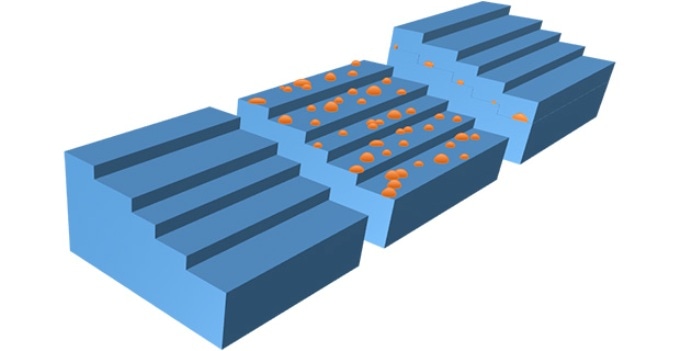
 Quantum dots (orange) form via self-assembly and nucleate randomly on the atomic steps of the semiconductor surface (blue). Credit: Boise State University
Next to silicon, germanium (Ge) is the most widely used semiconductor material in the world. While it is great at conducting electricity, Ge is inefficient at turning light into electricity or electricity into light, and this factor restricts its use in other applications.
Paul Simmonds, an assistant professor in the departments of physics and materials science and engineering, wanted to know if there was a way to modify the physical properties of germanium, and consequently improve its optoelectronic properties (how well it interacts with electronics and light)
The Air Force Office of Scientific Research was intrigued and provided a three-year, $622,000 grant to a proposal titled “Optoelectronic Properties of Strain-Engineered Germanium Dots”. Simmonds is collaborating on this project through a sub-award managed by the University of California, Los Angeles and the University of California, Merced. Boise State University’s share of the grant is $206,000.
If we can turn Ge into an optoelectronic material, then other characteristics would make it attractive as a laser material. It’s a bit like alchemy. We hope to change the fundamental properties of an element on the periodic table simply by stretching it a little.
Paul Simmonds, Assistant Professor, Boise State University
For many years, researchers have tried to put germanium under tensile strain (stretching it a little at the atomic level) to improve its optoelectronic properties. However, germanium is weak, and crystalline imperfections make it break even before tensile strain can build up.
As a response to this challenge, Simmonds and his collaborators have developed a new self-assembled nanomaterial family capable of storing tensile strain in large amounts, without damaging the crystalline structure.
Self-assembly has allowed us to develop a way for the materials to sustain high tensile strains without falling apart. Instead of remaining flat, the atoms rearrange to form nanoscopic islands, like raindrops on the top of a car but about a million times smaller. The process of rearranging into 3D islands relieves a little of the strain and creates a window that allows us to have high tensile strain without breaking any atomic bonds. We’ve shown this works with other materials and now we want to try it with germanium.
Paul Simmonds, Assistant Professor, Boise State University
This may help researchers establish tensile self-assembly as a new way to incorporate dissimilar materials, and demonstrate to the research community that nanostructure band produced with tensile strain can be an effective tool for detecting and designing materials for technological advancement.
Although developing direct band gap Ge nanostructures would be a significant breakthrough in optoelectronic materials research, Simmonds is happy that it’s also a chance to understand the world a little better.
The research team of Simmonds will perform the structural characterization and synthesis of the Ge nanostructures. Research collaborators from UCLA and UC Merced, who are well-known experts in optical spectroscopy and computational modeling, will help evaluate the materials developed at Boise State’s Collaboratory for Epitaxy of Nanomaterials.