Jul 1 2019
Atomically thin crystalline layers of transition metal dichalcogenides (TMDCs) have been grown by scientists from Tokyo Metropolitan University with different compositions over space, continuously feeding in various types of TMDC to a growth chamber to modify variations in properties.
Examples consist of 20 nm strips surrounded by various TMDCs with atomically straight interfaces, and layered structures. They also directly investigated the electronic properties of these heterostructures; probable applications include electronics with unmatched power efficiency.
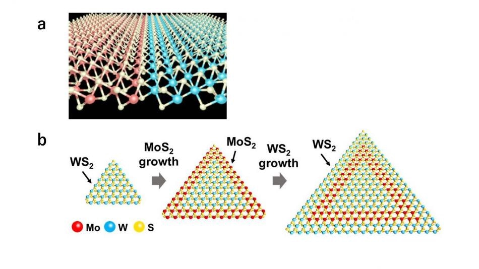
 (a) Red and blue are different metal atoms; yellow is chalcogen atoms. (b) Newly developed procedure. Different TMDC precursors are fed in sequentially to grow crystalline domains with different composition. (Image credit: Tokyo Metropolitan University)
Semiconductors are essential in the contemporary period; silicon-based integrated circuits support the operation of everything that is digital, from discrete devices such as smartphones, computers, and home appliances to regulate components for all kinds of imaginable industrial applications.
A wide range of scientific research has been aimed at the next steps in semiconductor design, mainly the application of novel materials to design more compact, efficient circuitry which makes use of the quantum mechanical behavior of materials at the nanoscale. Of particular interest are materials with a primarily different dimensionality; the most well-known example is graphene, a 2D lattice composed of carbon atoms which is atomically thin.
Transition metal dichalcogenides (or TMDCs) are favorable options for adding into new semiconductor devices. Made up of transition metals like tungsten and molybdenum and a chalcogen (or Group 16 element) like selenium or sulfur, they can develop layered crystalline structures whose properties vary significantly when the metallic element is modified, from regular metals to semiconductors, even to superconductors.
By controllably intertwining domains of various TMDCs into a single heterostructure (composed of domains with distinct composition), it may be feasible to create atomically thin electronics with distinct, enhanced properties to current devices.
A research team guided by Dr. Yu Kobayashi and Associate Professor Yasumitsu Miyata from Tokyo Metropolitan University has been at the vanguard of efforts to develop 2D heterostructures with various TMDCs using vapor-phase deposition, the deposition of precursor material in a vapor state onto a surface to create atomically flat crystalline layers. One of the toughest challenges they faced was developing a seamlessly flat interface between different domains, a vital feature for making the most out of these devices.
Now, they have been successful in formulating a continuous process to grow distinct crystalline strips of different TMDCs at the edge of current domains, producing strips as thin as 20 nm with a different composition.
Their new method uses liquid precursors which can be fed into a growth chamber in sequence; by enhancing the growth rate, they were able to grow heterostructures with different domains connected flawlessly over atomically straight edges. They directly imaged the connection using scanning tunneling microscopy (STM), finding exceptional agreement with first-principles numerical simulations of what a perfect interface should resemble. The team used four types of TMDCs, and also realized a layer-on-layer heterostructure.
By producing atomically sharp interfaces, electrons may be successfully confined to one-dimensional spaces on these 2D devices, for perfect control of electron transport and resistivity as well as optical properties. The researchers anticipate that this may make way for devices with unmatched energy efficiency and unique optical properties.