Nov 13 2019
At the University of Cambridge, researchers focused on perovskite materials for flexible LEDs and sophisticated solar cells have found that these materials can be more efficient when they have less ordered chemical compositions. This discovery can considerably simplify manufacturing processes and reduce related costs.
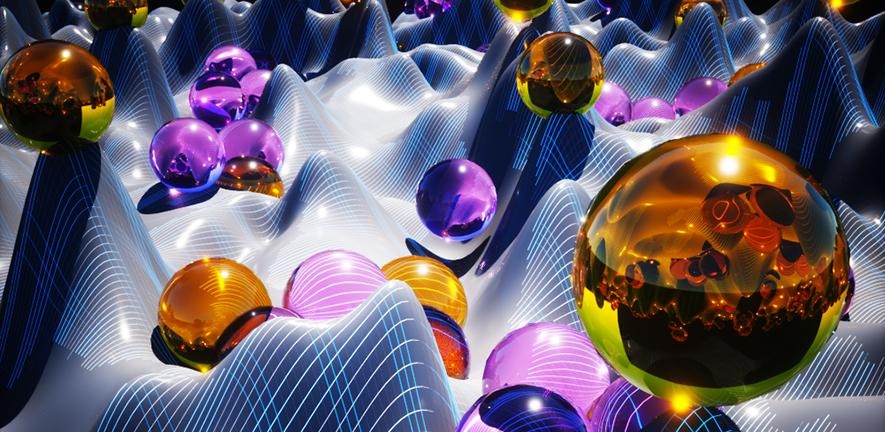
 Artist’s impression of perovskite structures. Image Credit: Ella Maru Studio.
Published in Nature Photonics, this unexpected discovery is the outcome of a collaborative study headed by Dr Felix Deschler and Dr Sam Stranks.
Crystalline silicon is a material that is often used for creating solar panels. However, a costly and time-intensive production process is required to efficiently convert energy. In addition, the wafer structure of the silicon material needs to be highly ordered, and the material itself is rather sensitive to dust and other impurities. Hence, it should be made only in a cleanroom.
Despite these challenges, perovskite materials have evolved as potential alternatives in the last 10 years.
The lead salts utilized for making these materials are not only more abundant but can also be produced more cost-effectively when compared to crystalline silicon. These salts can be prepared in a liquid ink that can be easily printed to create a film of the material.
The components utilized for making the perovskite materials can be modified to give different structural properties and colors to the materials—for instance, the films can be made to produce different colors, or harvest sunlight in a more efficient way.
Only a thin film of this perovskite material is required—about a thousand times thinner than a single strand of a human hair—to achieve efficiencies similar to the silicon wafers being used today. This provides new opportunities to use this material in ultra-lightweight, flexible smartphone screens or windows.
This is the new class of semiconductors that could actually revolutionise all these technologies. These materials show very efficient emission when you excite them with energy sources like light or apply a voltage to run an LED.
Sascha Feldmann, PhD Student, Cavendish Laboratory, University of Cambridge
Feldmann continued, “This is really useful but it remained unclear why these materials that we process in our labs so much more crudely than these clean-room, high-purity silicon wafers, are performing so well.”
Earlier, researchers had believed that if the materials are made to have a more ordered structure, they would be more efficient just like silicon materials. However, Feldmann and Stuart MacPherson—her co-lead author—were surprised to note that the reverse was true.
The discovery was a big surprise really. We do a lot of spectroscopy to explore the working mechanisms of our materials, and were wondering why these really quite chemically messy films were performing so exceptionally well.
Dr Felix Deschler, Cavendish Laboratory, University of Cambridge
Deschler is currently leading an Emmy-Noether research team at TU Munich.
“It was fascinating to see how much light we could get from these materials in a scenario where we’d expect them to be quite dark,” stated MacPherson, a PhD student in the Cavendish Laboratory. “Perhaps we shouldn’t be surprised considering that perovskites have re-written the rule book on performance in the presence of defects and disorder.”
The scientists found that their rough and multi-component alloyed preparations were, in fact, boosting the materials’ efficiency by producing plenty of areas that have different compositions. These compositions can capture the energized charge carriers—either from an electrical current in an LED, or sunlight in a solar cell.
“It is actually because of this crude processing and subsequent de-mixing of the chemical components that you create these valleys and mountains in energy that charges can funnel down and concentrate in,” added Feldmann. “This makes them easier to extract for your solar cell, and it’s more efficient to produce light from these hotspots in an LED.”
The researchers’ findings can have a major impact on the production success of the perovskite materials.
“Companies looking to make bigger fabrication lines for perovskites have been trying to solve the problem of how to make the films more homogenous, but now we can show them that actually a simple inkjet printing process could do a better job,” Feldmann further stated.
He continued, “The beauty of the study really lies in the counterintuitive discovery that easy to make does not mean the material will be worse, but can actually be better.”
“It is now an exciting challenge to find fabrication conditions which create the optimum disorder in the materials to achieve maximum efficiency, while still retaining the structural properties needed for specific applications,” added Dr Deschler.
If we can learn to control the disorder even more precisely, we could expect further LED or solar cell performance improvement—and even push well beyond silicon with tailored tandem solar cells comprising two different colour perovskite layers that together can harvest even more power from the sun than one layer alone.
Dr Sam Stranks, University Lecturer in Energy, Department of Chemical Engineering and Biotechnology, Cavendish Laboratory, University of Cambridge
Perovskite materials are also sensitive to moisture, which is another drawback. Hence, the researchers are also exploring ways to enhance the stability of these materials.
“There’s still work to do to make them last on rooftops the way silicon can—but I’m optimistic,” concluded Stranks.