Mar 10 2020
A research team from the National University of Singapore (NUS) has developed a new set of reconfiguration methods that adaptively extends the least consumption of power as well as the highest performance of digital circuits, much beyond the standard voltage scaling.
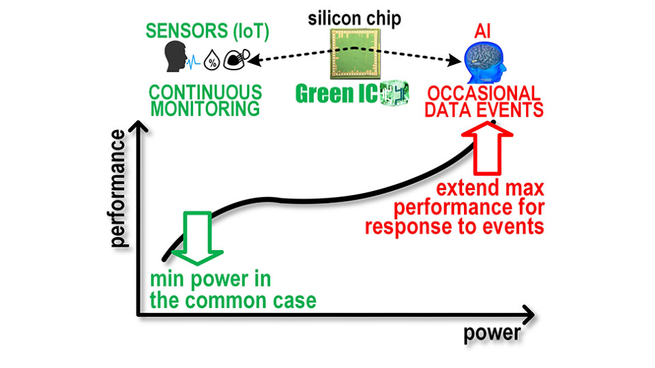
 The adaptive digital circuits demonstrated by the NUS team are able to extend the battery life of intelligent silicon chips by reducing the power consumption under normal use, while scaling up performance to quickly respond to occasional data events. Image Credit: National University of Singapore.
Extended adaptation like this enables digital silicon chips to work at lower power during regular use and also to operate at a higher performance level, if required.
This prolongs the life of the batteries under the tentative availability of power in systems driven by rechargeable batteries or harvesters (for example, solar cells) and, at the same time, delivers greater peak performance to perform on-chip data analytics following the occurrence of specified events. This is the most important enabler for several applications, like artificial intelligence (AI), Internet of Things (IoT), biomedical devices, and wearables.
Our reconfiguration techniques introduce unprecedented adaptability to fluctuating power availability and performance demand. Compared to the industry-standard voltage scaling technique, measurements on several test chips in our lab have shown that such adaptation extends the battery life of a mobile or wearable device by 1.5 times, while doubling peak performance.
Massimo Alioto, Associate Professor, NUS Engineering, National University of Singapore
Alioto continued, “Our techniques can also be used to further miniaturise the battery by the same factor, while maintaining the same battery life.”
Alioto is also the leader of the NUS Green IC Group that contributed to this technological innovation.
“As further benefit, the power-performance versatility of our circuit techniques allows semiconductor companies to simplify their chip portfolio and reduce the design cost, as the same digital design can be reused across a wide range of applications and markets,” he further added.
The suggested methods have resulted in the demonstration of processors (for instance, Fast Fourier Transform, ARM processors) and accelerators with the least consumption of energy reported to date.
The study behind the new class of reconfiguration methods was supported by top semiconductor firms (TSMC and Intel) and also by the National Research Foundation of Singapore and the Singapore Ministry of Education.
Data and Clock Path Adaptation: Achieving Both Low Minimum Power Consumption and Higher Peak Performance
A majority of the sophisticated mobile, AI, and IoT applications need a broad and flexible trade-off between the average power (that is, the lifespan of batteries) and the highest performance level that determines the responsiveness of the system (for example, when the screen is touched, or carrying out data analytics when a sensor generates the required data).
Presently, dynamic voltage scaling is the established standard in allowing such flexibility. Functioning at voltages of about 1 V results in maximum performance level and the highest consumption of energy, while reduction as low as 0.4 to 0.5 V slows the operating rate by almost 10 times and reduces the consumption of energy by as much as four to five times.
However, this method has one disadvantage: voltage scaling is normally applicable to a fixed digital architecture, albeit the optimal architecture meant for performance and energy consumption relies on the adopted voltage.
The invention made by NUS researchers surpasses voltage scaling because its circuit reconfiguration allows a better match between the adopted voltage and the architecture. This results in more reduction in energy usage as well as improved performance levels at varied voltages.
Our invention enables reconfiguration of both the ‘data path’ where the actual processing is performed, and the ‘clock path’ that distributes the clock signal to orchestrate the different processing tasks. In both cases, their fundamental building blocks are flexibly merged or split to create the data and clock path structure that improves either energy efficiency or performance at a given voltage.
Massimo Alioto, Associate Professor, NUS Engineering, National University of Singapore
When compared to traditional voltage scaling, the method recommended by the NUS Green IC team renders digital circuits more adaptive and versatile, thus enabling concurrent optimization at the two ends of the power-performance spectrum.
Technical Book and a Complete Toolchain Publicly Available
A technical book has now been issued to share the advantages of the scientists’ latest method with both research groups and industry across the world. This book gives details and background of the silicon chip implementation of accelerators, processors, and on-chip memories. In addition, an automated design flow has been developed and publicly launched over GitHub.
In our book, we introduced and demonstrated design methodologies using solely commercial design tools, which are integrated into a cohesive design flow where clock and data path reconfiguration is incorporated in a plug-and-play fashion. We are delighted to share the software code in an open-source fashion to enable massive and rapid adoption of our novel techniques in the commercial sector and in academic research.
Massimo Alioto, Associate Professor, NUS Engineering, National University of Singapore
Next Steps
At present, the NUS researchers are looking for ways to develop new sets of smart silicon systems that enable ultra-wide power-performance adaptation in AI accelerators that are integrated into sensing silicon chips for IoT applications.
Such an approach will result in sophisticated systems that are constantly available and, at the same time, can quickly act in response to external events with extremely important computational performance.
In their study, the researchers strive to allow power-performance adaptation via design methodologies and drop-in methods in current system architectures. This makes it possible to achieve power-performance advantages without affecting the design ecosystem and thus allows a large and fast adoption of next-generation intelligent systems.