Reviewed by Alex SmithAug 18 2021
A new approach has been discovered by physicists to create transistors by making use of materials that are acclaimed for their performance in next-generation light-emitting diodes (LEDs) and solar cells.
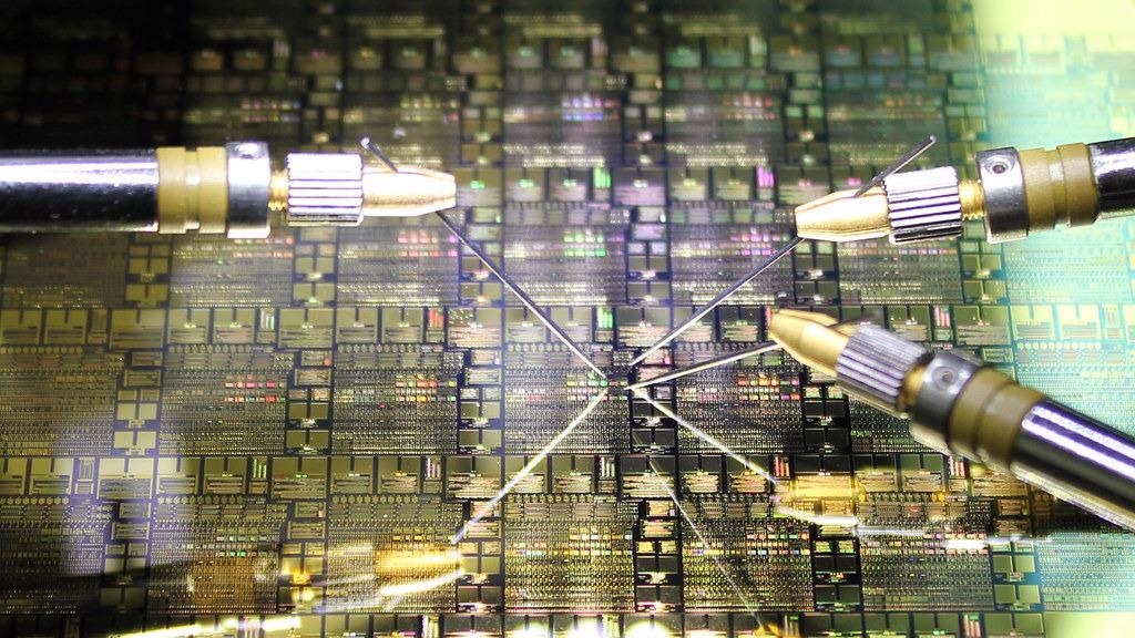
 Scientists make transistors using perovskite, overcoming a long-standing ion obstacle. Image Credit: University of Bath.
The scientists have overcome the issue of the material’s ion content meddling with the flow of electronic current through a transistor. This discovery might open the door for studies into greener electronic components for affordable electronic devices.
In the last 10 years, solution-processed metal-halide perovskites (a hybrid metal-organic material) have been a center point of study into economical, high-efficiency solar cells and LEDs.
Perovskites exhibit the potential to process at comparatively low temperatures and are, therefore, regarded as a greener alternative to silicon, not only for the fabrication of solar cells but also for transistors. A transistor is considered to be the building block of an integrated circuit and the primary component in many electronic devices.
Transistors function via a gate system: electrons flow between a “source” and a “drain,” and their flow is regulated by an electric field applied to the “gate.” The occurrence of ions in a transistor hinders the flow of electronic current, making the transistor unworkable.
Metal-halide perovskites are rich in ions. On applying an electric field to a perovskite, these ions respond to the electric field by rushing to the gate and piling up there. This effectively blocks the electron flow between the source and the drain.
To overcome this interference, researchers have spent the last 10 years looking for approaches to stymie the ions, which would help manipulate them to reduce their detrimental effects on the perovskite transistor.
Researchers from the University of Bath and the Max Planck Institute for Polymer Research (MPIP) in Germany have discovered a solution to the perovskite issue. This allows the material to function as a transistor at room temperature.
The device has been “tricked” into overlooking the ion content of the material by bypassing such electrically charged species away from the gate to a different part of the transistor, where they cannot interfere with the current flow.
Until now, the presence of ions in perovskites has rendered the use of perovskites in transistors challenging. We saw this as a shame since perovskites are very promising semiconducting materials.
Kamal Asadi, Study Lead Researcher Professor, Department of Physics, University of Bath
Asadi continued, “At room temperature, the perovskite’s ions are pretty mobile. People have resorted to reducing the temperature to get perovskite transistors to work because at low temperatures, ions are less mobile. But in real-life applications, that would mean that our perovskite-based gadgets would only operate reliably in the fridge or in Antarctica.”
“We looked at the problem from a different angle. We modified the construction of the transistors instead of modifying the material, resulting in a transistor with an extra, auxiliary gate. Ions are then pushed to the auxiliary gate and fixed in position. Then, when you apply a gate electric field, the electrons now see the gate field, react to it, and an electron flow between the source and the drain is established,” added Asadi.
The researchers deposited a ferroelectric layer onto the transistor to create the auxiliary gate. Ferroelectrics are dielectric materials that exhibit stable polarization when the external electric field is shut down. They can stimulate a huge surface charge that attracts ions and retains them in position, thus clearing the gate for electron flow. The Bath researchers are the first to mitigate ion transport by using the concept of ferroelectricity.
Pushing the ions away from the transport channel can only be achieved with auxiliary gate materials that can induce large surface charges, such as ferroelectrics or electrolytes. We chose ferroelectric polymers because of their compatibility and ease of processing on top of the perovskite layer.
Dr Beomjin Jeong, Study First Author, Max Planck Institute for Polymer Research
The researchers involved in this project expect extensive interest in the platform that they have developed, with other scientists broadening the hunt for materials with a high surface charge density that can be coupled with perovskite.
A right level of control over ions in the transistor channel achieved by a ferroelectric layer would be useful for other applications where there is a necessity for concurrent control of electrons and ions.
Journal Reference:
Jeong, B., et al. (2021) Room-Temperature Halide Perovskite Field-Effect Transistors by Ion Transport Mitigation. Advanced Materials. doi.org/10.1002/adma.202100486.