Scientists from Columbia University’s Department of Mechanical Engineering have reported an innovative approach for embedding active electronic components into devices during selective laser printing, an additive manufacturing process. Their findings have appeared in the journal Additive Manufacturing Letters.

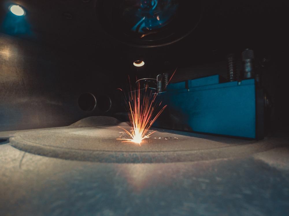
Study: Embedding Components During Laser Sintering. Image Credit: MarinaGrigorivna/Shutterstock.com
Embedding Active Components into Devices with Additive Manufacturing
Additive manufacturing provides several industries with powerful tools to design devices with minimum waste and processing steps. In the field of electronics, these manufacturing processes offer the ability for components to be embedded in devices by stopping the print, incorporating the component into voids in the printed material, and carrying on the print.
Embedding components into printed materials converts them from passive parts to active systems. A wide range of components can be incorporated into parts in this manner, including mechanical and electronic parts. These can include batteries and energy storage devices, actuators, motors, chips, and sensors. Fasteners, wires, linkages, and stiffeners can be incorporated to increase the strength of parts or shorten the time needed to produce useful devices post-print.

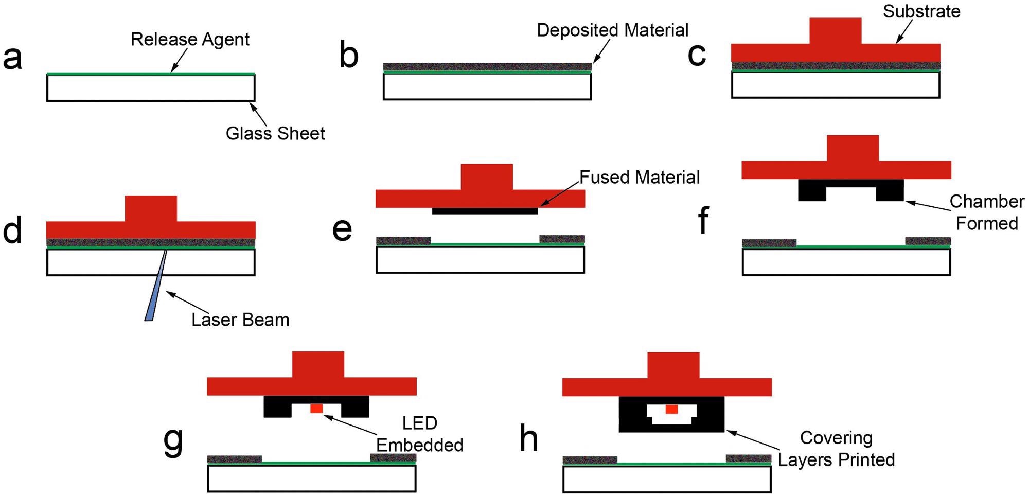
a) The selected release agent is coated onto the glass b) The release agent fluidically captures a single powder material layer c) Substrate is pressed onto the upper surface of the powder d) The laser fuses a selected region of powder to the substrate e) The substrate is raised with the fused powder, the glass is then recoated with a new layer of powder f) The process continues, with several initial base layers and chamber layers being formed g) An LED with wires soldered to it is embedded in the powder chambers, the wires lead out of an open region in the walls of the chamber h) Several capping layers are added to finish embedding the print, there is still a small hole in the side of the chamber regions for the wires to protrude from. Image Credit: Whitehead, J & Lipson, H et al., Additive Manufacturing Letters
Problems with Component Embedding Using Sintering Methods
Selective laser sintering is one additive manufacturing process that has been explored for printing electronic devices with embedded components. Standard sintering processes construct parts out of homogenous layers of unfused powder and then use a laser to selectively sinter this micron-scale powder to produce the final product.
Embedding components into sintered parts is challenging, limiting the suitability of this process for producing functionalized devices. When each layer is deposited, the laser fuses it to the previously printed layer, with the unfused powder remaining in the print bed and acting as a support for the printed part, making it difficult to include voids for component placement.
Some techniques have been developed in recent years to overcome these issues, with limited success and challenges of their own. Placeholder objects can be printed and replaced, but this requires additional mechanisms, which increases print complexity. Powder may fall into gaps surrounding the component if the embedded component’s tolerance is not high enough.
Covering layers may be uneven and fusing the component to the rest of the printed part can be challenging. Moreover, laser penetration, contact with heated materials, and powder contamination may damage the embedded component if it is in contact with the covering layer.
The Study
The authors have proposed a novel sintering process that overcomes these issues and facilitates the efficient printing of parts with embedded electronic and mechanical components. The process proposed by the authors is termed inverted laser sintering.
The novel approach is similar to conventional selective laser printing, with one crucial difference. In inverted laser sintering, a thin layer of powder is first deposited onto a glass sheet. Then, a substrate is pressed onto the upper layer of the material. A laser is then directed upwards through the bottom of the glass sheet, and a region of the powder layer can be selectively sintered.
By raising the substrate and replenishing the material, layers can be fused to each other using laser sintering without the need for passive powder support, overcoming the reported issues with embedding components into printed devices using conventional laser sintering.
This process confers several advantages over conventional methods. Firstly, the lack of surrounding powder allows operators to see the printed part more clearly, enabling earlier fault detection. Additionally, multi-material printing is easier than standard selective laser sintering processes.
However, the biggest advantage of not using a print bed is that it allows components to be embedded once the print is stopped, and then depositing the next layer and covering the hollow void without powder layers covering the part and limiting its functionality or complicating the print process. Placeholder parts are not needed, avoiding the issues associated with using them.
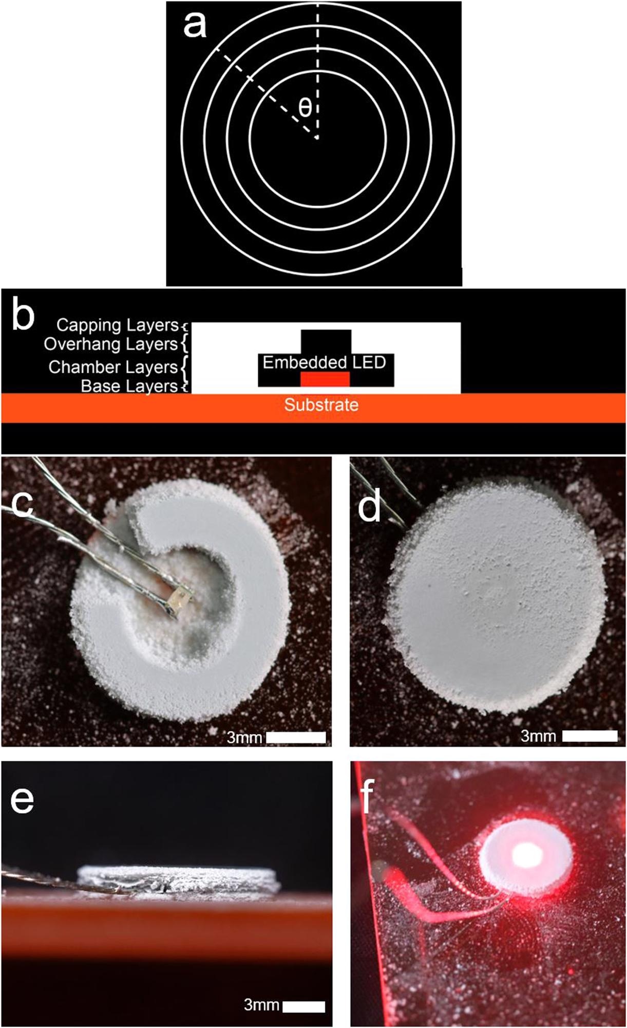
The authors demonstrated the suitability of inverted laser sintering to produce printed active electronic systems by fabricating a thermoplastic component with an embedded light-emitting diode.

a) Diagram of nested circle layer sintering pattern b) Layer diagram for the embedded LED sample c) Embedded LED adhered to the base layers, surrounded by material in the chamber layers d) Upper surface of the embedded LED sample e) Side view of the embedded LED sample showing the wires f) Activated LED shining through the upper surface of the sample. Image Credit: Whitehead, J & Lipson, H et al., Additive Manufacturing Letters
In Summary
The paper has demonstrated the successful printing of parts with embedded electronic components using inverted laser sintering. This novel additive manufacturing technique overcomes many of the issues with conventional laser sintering. Whilst the authors demonstrated the process’s suitability by printing a simple electronic component, they have stated that inverted laser sintering can print more complex functional parts for a variety of electronic devices.
As well as incorporating voids for embedded components, the process could print channels to connect different device elements. It is even possible to incorporate channels and components in different layers, opening the possibility of printing multi-dimensional electronic circuits. Moreover, these printed parts require fewer post-processing assembly steps. The authors will be undertaking further work on printing embedded components with connected wires.
Further Reading
Whitehead, J & Lipson, H (2022) Embedding Components During Laser Sintering Additive Manufacturing Letters 100055 [online, pre-proof] sciencedirect.com. Available at: https://www.sciencedirect.com/science/article/pii/S2772369022000299?via%3Dihub
Disclaimer: The views expressed here are those of the author expressed in their private capacity and do not necessarily represent the views of AZoM.com Limited T/A AZoNetwork the owner and operator of this website. This disclaimer forms part of the Terms and conditions of use of this website.