May 5 2015
Researchers at Berkeley Lab have discovered one-dimensional, topologically protected ballistic electron conducting channels at bilayer graphene’s domain walls.
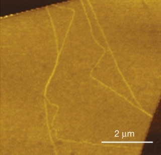
 In this near-field infrared nanoscopy image of bilayer graphene obtained at the Advanced Light Source, domain walls are revealed by bright lines that arise because of the walls’ electronic structures and IR responses.
These electron conducting channels could be used as electron valley polarization filters in quantum computers, and other such devices as they are “valley polarized”.
This discovery enables utilization of valleytronics for potential applications using graphene. Valleytronics is data coding in electron’s wavelike motion when it travels through a conductor.
Graphene is a material that is faster and stronger than silicon. It is made up of pure carbon and is a two-dimensional semiconductor.
“Combining near-field infrared nanometer-scale microscopy and low-temperature electrical transport measurements, we have recorded the first experimental observations of 1D ballistic electron conducting channels at bilayer graphene domain walls,” says Feng Wang, a condensed matter physicist with Berkeley Lab’s Materials Sciences Division, who led this work.
“These 1D valley-polarized conducting channels featured a ballistic length of about 400 nanometers at 4 kelvin. Their existence opens up opportunities for exploring unique topological phases and valley physics in graphene.”
Valleytronics is considered to hold significant promise for quantum computing, and hence considerable interest exists in the high-tech industry. Conventionally, electrical charges are used in classical electronics for data processing. In the same way as spintronics, valleytronics provides an enormous advantage in terms of speeds for data processing.
A paper about this research has been published in the journal Nature. Wang is the corresponding author of this paper, and he holds an appointment with the Berkeley Physics Department at the University of California. The lead authors of the paper are Zhiwen Shi and Long Ju, who are part of Wang’s research group.
“In valleytronics, electrons move through the lattice of a 2D semiconductor as a wave with two energy valleys, each valley being characterized by a distinct momentum and quantum valley number,” Wang says. “This quantum valley number can be used to encode information when the electrons are in a minimum energy valley.”
Theoretical work that had been conducted recently suggests that 1D electron conducting channels required for valleytronics could be realized at the domain walls between BA- and AB- stacked bilayer graphene. The atomic defects that exist at the edges of graphene lead to valley-mixing; however, the domain walls are smooth and can help preserve the electron valleys.
The facilities at Berkeley Lab’s Advanced Light Source (ALS) were utilized by the research team. They successfully imaged in situ bilayer graphene layer-stacking domain walls on device substrates using tightly focused infrared light beams. The 1D conducting channels were revealed when field effect devices were created over these domain walls.
“The infrared measurements were carried out at ALS beamline 5.4,” says Shi. “The near-field infrared capabilities of this beamline enable optical spectroscopy with spatial resolutions that are way beyond the diffraction limit, allowing us to image the nanometer-wide domain walls in bilayer graphene.”
Most research that has been conducted on valleytronics till now has concentrated on MX2 materials, which are 2D semiconductors. These materials are made up of a single transition metal atom layer that is sandwiched between two chalcogen atom layers. Sulfur is a chalcogen, while tungsten or molybdenum is used in the transition metal layer.
This study proves that it is possible to realize protected topological phases in bilayer graphene, which would enable 2D carbon sheets to be used for valleytronic applications.
“Our next step is to increase the ballistic length of these 1D channels so we can utilize them as electron valley filters, as well as for other manipulations of electron valleys in graphene,” Wang says.