Aug 1 2017
Researchers have recently found out that a collective rattling effect in a form of crystalline semiconductor prevents much of the heat transfer and preserves high electrical conductivity. According to the Researchers, this is a rare combination with the ability to minimize the accumulation of heat in electronic devices and turbine engines, apart from other prospective applications.
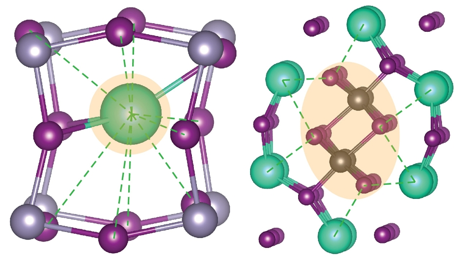
 Rattling structures of halide perovskites: cesium tin iodide (left) and cesium lead iodide (right). CREDIT: Berkeley Lab/UC Berkeley.
A team headed by Researchers from the Department of Energy’s Lawrence Berkeley National Laboratory (Berkeley Lab) unearthed these striking properties in a family of materials called halide perovskites, which are believed to be favorable for futuristic electronic displays, solar panels, electronic cooling and nanoscale lasers.
These interdependent thermal and electrical characteristics, that is, “thermoelectric” characteristics, were observed in nanoscale wires made of cesium tin iodide (CsSnI3). The material was found to possess the lowest level of heat conductivity amid materials that have a continuous crystalline structure.
According to the Scientists, when compared to conventional thermoelectric materials like silicon-germanium, this mono-crystal material can be more readily synthesized in huge amounts.
Its properties originate from the crystal structure itself. It’s an atomic sort of phenomenon.
Woochul Lee, a Postdoctoral Researcher at Berkeley Lab and Lead Author of the study
The study was reported in the Proceedings of the National Academy of Sciences on 31st July 2017. These are the initially reported outcomes regarding the thermoelectric performance of this mono-crystal material.
Prior to this, Scientists were of the view that the thermal characteristics of the material were due to the rattling of “caged” atoms inside the crystalline structure of the material, as noticed in yet other materials. The rattling can assist in interrupting the transfer of heat in a material.
We initially thought it was atoms of cesium, a heavy element, moving around in the material.
Peidong Yang, a Senior Faculty Scientist at Berkeley Lab’s Materials Sciences Division who headed the study
Jeffrey Grossman, a Scientist from the Massachusetts Institute of Technology, then carried out some theoretical study and computerized simulations that helped to explain the observations of the research team. The team also employed Berkeley Lab’s Molecular Foundry, specializing in nanoscale study, for this research.
“We believe there is essentially a rattling mechanism, not just with the cesium. It’s the overall structure that’s rattling; it’s a collective rattling,” stated Yang. “The rattling mechanism is associated with the crystal structure itself,” and is not caused due to the clustering of tiny crystal cages. “It is group atomic motion,” further stated Yang.
Inside the crystal structure of the material, the distance from one atom to another is decreasing and increasing in a collective manner such that the heat is prevented from being transferred easily.
However, as the structure of the material is made up of an orderly and mono-crystalline, electrical current can still pass through the material in spite of the collective rattling. Its electrical conductivity is similar to a submarine moving smoothly in placid underwater currents. In contrast, its thermal conductivity is similar to a sailboat traveling on the surface of rough seas.
According to Yang, two main uses of thermoelectric materials are in the areas of cooling and transforming heat into electrical current. Specifically in the case of CsSnI3, cooling functionalities, for instance, a coating to assist in cooling electronic camera sensors, can be easily realized as against heat-to-electrical transformation, added Yang.
A major difficulty is that the material is extremely reactive to water and air, hence it necessitates an encapsulation or protective coating to be able to operate inside a device.
According to Yang, CsSnI3 was initially ascertained as a semiconductor many years ago. However, only recently has it been revealed again for its various distinctive properties. “It turns out to be an amazing gold mine of physical properties,” noted Yang.
In order to compute the thermal conductivity of the material, the research team connected a CsSnI3 nanowire at either end to micro-islands of an anchoring material, where the micro-islands acted as both a thermometer and a heater. The team heated one micro-island and accurately computed the manner in which the nanowire conveyed heat to the other island.
They also employed scanning electron microscopy to accurately measure the nanowire’s dimensions, which were used to compute a precise measure of the thermal conductivity of the material. The Researchers repeated the experiment using multiple disparate nanowire materials and different nanowire samples to compare thermoelectric characteristics and validate the thermal conductivity computations.
A next step is to alloy this (cesium tin iodide) material. This may improve the thermoelectric properties.
Woochul Lee, a Postdoctoral Researcher at Berkeley Lab and Lead Author of the study
Moreover, similar to the manner in which Computer Chip Manufacturers inject a series of elements into silicon wafers to enhance their electronic characteristics, or namely “doping,” Researchers aspire to use similar methods to thoroughly use the thermoelectric properties of this semiconductor material. According to Yang, this is a comparatively uninvestigated domain for this type of materials.
Other Scientists from Berkeley Lab’s Materials Sciences Division and the Molecular Foundry, the Kavli Energy NanoScience Institute at UC Berkeley and Berkeley Lab, and UC Berkeley’s Department of Chemistry were part of the research team.
The Molecular Foundry is a DOE Office of Science User Facility that offers free access to ultra-modern equipment and multidisciplinary proficiency in nanoscale science to visiting Researchers from all across the globe.
The Department of Energy’s Office of Basic Energy Sciences supported the study.