Feb 1 2016
Computer chips are currently built by stacking layers of varied materials and engraving patterns into them.
A report on the very first chip fabrication method developed by a team of MIT researchers was published in a recent issue of Advanced Materials. This new method allows varied materials to be deposited in the same layer. The report also highlights that the same method was used to create chips with working versions of all of the circuit components necessary to build a general-purpose computer.
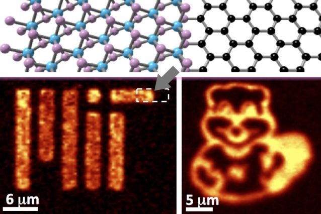
 Researchers used the MIT and Tim the Beaver logos to show photoluminescence emissions from a monolayer of molybdenum disulfide inlayed onto graphene. The arrow indicates the graphene-MoS2 lateral heterostructure, which could potentially form the basis for ultrathin computer chips. (Courtesy of the researchers)
Very thin material layers were used in their experimental chip, each layer was between one and three atoms thick. This research could support the efforts to develop transparent, flexible, and thin computing devices, which could be laminated on to a wide range of materials.
The methodology is universal for many kinds of structures. This offers us tremendous potential with numerous candidate materials for ultrathin circuit design.
Xi Ling, Postdoc, Research Laboratory of Electronics
This method could also effect the development of the high-speed, ultralow-power computing devices referred to as tunneling transistors. The method also helps to incorporate optical components into computer chips.
It’s a brand new structure, so we should expect some new physics there.
Yuxuan Lin, Graduate Student, Electrical Engineering and Computer Science
Ling and Lin are joined on the paper by Mildred Dresselhaus, an Institute Professor emerita of physics and electrical engineering; Jing Kong, an ITT Career Development Professor of Electrical Engineering; Tomás Palacios, an associate professor of electrical engineering; and by another 10 MIT researchers and two more from Brookhaven National Laboratory and Taiwan’s National Tsing-Hua University.
Crystalline solids are used to create computer chips. The atoms of these materials are positioned in a geometrical pattern called a crystal lattice. Previously materials with very similar lattices were laterally deposited in the same chip layer, however the team’s experimental chip makes use of two materials with varied lattice sizes (molybdenum disulfide and the single-carbon-atom-thick material graphene).
The team’s fabrication technique is applicable for all materials, like molybdenum disulfide, which incorporates elements from group six of the periodic table, such as tungsten, molybdenum, and chromium, and also elements from group 16, which include tellurium, selenium, and sulfur. These compounds are mainly semiconductors, which play a vital role in transistor design. The compounds are also useful in very thin layers.
The second material, graphene is known to be the strongest material, and also has the highest electron mobility, a measure of how quickly electrons move through it. Graphene is best used in thin-film electronics, or a number of nanoscale electronic devices.
To assemble the laterally integrated circuits, graphene is deposited on a solicon substrate. It is then etched away in the areas where molybdenum disulfide is to be deposited.
A solid bar of PTAS is then placed at one of the substrate’s ends, it is heated and a gas flows through it and across the substrate. PTAS molecules present in the gas do not stick to the graphene, but only stick to the silicon that is exposed. Every time the PTAS molecules stick, they cause a reaction with a different gas that leads to the formation of a molybdenum disulfide layer.
In an earlier study, a wide variety of materials were identified by the researchers to promote the development of crystals belonging to several other compounds, and it is possible to include any one of these materials into the process.
More powerful computing can be obtained if this new fabrication method is used to develop tunneling-transistor processors.A transistor can be adjusted to stop a charge from crossing, or to allow it pass through a barrier. However, in a tunneling transistor a counterintuitive quantum-mechanical effect allows the charge to cross the barrier. In this effect, an electron is considered to disappear at one particular location and then reappear at another location.
All of these effects are a lot more pronounced at very small scales, such as the one- to three-atom thicknesses of the experimental chip’s layers. The tunneling transistors can function under extremely low power, and also gain higher speeds because the electron tunneling is not affected by the thermal phenomena limiting the efficiency of traditional transistors.
This work is very exciting. The MIT team demonstrated that controlled stitching of two completely different, atomically thin 2-D materials is possible. The electrical properties of the resulting lateral heterostructures are very impressive.
Philip Kim, Physics Professor, Harvard University