AFSEM is an atomic force microscope (AFM) designed for use within an SEM or Dualbeam (SEM/FIB) microscope. Its open-access design allows for simultaneous operation of both SEM and AFM within the same vacuum chamber to provide correlated AFM and SEM imaging, enabling a deeper, more detailed analysis of your sample.
AFSEM opens up new possibilities for exploring the micro and nano worlds by combining these complementary techniques
Achieve high-resolution imaging, create 3D topographic maps, and accurately measure features like heights, distances, and material properties while maintaining the broad field of view of the SEM, offering the flexibility to precisely position the AFM cantilever where it's needed. The AFSEM’s intuitive software makes system operation, measurement, and data analysis efficient and straightforward.
For material and product analysis, multiple techniques are often important to explore different parameters and identify correlations. AFSEM simplifies correlative SEM-AFM analysis by allowing you to measure the same area with both techniques directly within the SEM, ensuring precise alignment and enhanced insight.
Download the Brochure for More Information
AFSEM Features
- Small size; does not hinder SEM operation
- Several different measurement modes available
- Uses self-sensing cantilevers
- Strong, user-friendly control software
- Compatible with most SEMs/FIBs
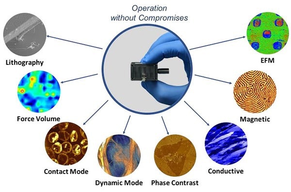
Image Credit: Quantum Design, Inc.
The AFSEM is a fully complete atomic force microscope that performs all the typical measurement modes anticipated from a typical AFM. The controller software allows the user to effortlessly select between contact mode, intermittent contact mode, non-contact mode, force-volume mode, and phase contrast mode.
Using the functional probes, the advanced modes—electrostatic force microscopy (EFM_, magnetic FM (MFM), and conductive AFM (C-AFM)—are also accessible. Kelvin probe FM (KPFM) and Scanning Thermal Microscopy (SThM) are being developed.
Measurement Modes
Standard AFM
When in contact mode, the tip touches the sample’s surface, closely following the topography in the repulsive regime. Long, soft cantilevers with low force constants are employed for contact mode.
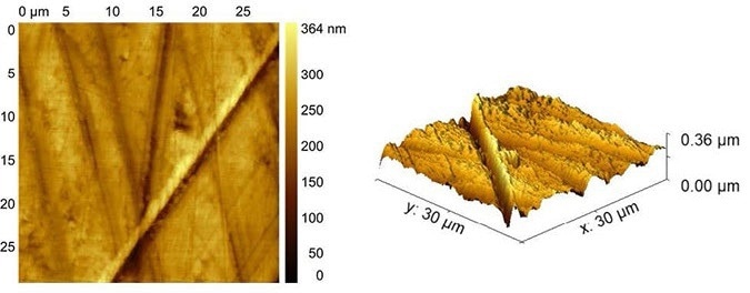
(Figures 1 and 2) AFSEM image of a polymer surface obtained in contact mode. Image Credit: Quantum Design, Inc.
The cantilever oscillates close to its resonance frequency in intermittent contact mode, also known as dynamic mode. The interaction between the tip and the sample causes the oscillation's amplitude to fluctuate as the tip approaches the surface. A predetermined cantilever oscillation amplitude is maintained by adjusting the height while the cantilever scans across the sample. The force of the tip’s sporadic interactions with the surface is imaged to create an AFM image.
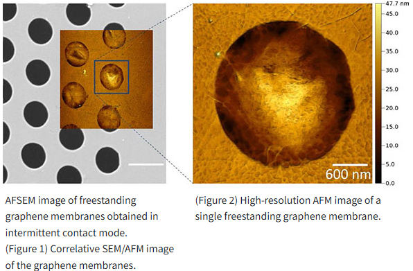
Image Credit: Quantum Design, Inc.
The cantilever’s tip does not touch the sample surface in non-contact mode. As the tip only oscillates with a very little amplitude and is only impacted by long-range pressures, neither sample nor tip deterioration occurs.
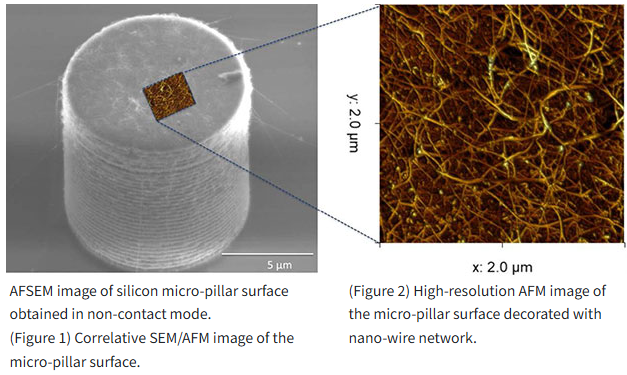
Image Credit: Quantum Design, Inc.
Topographic imaging and force measurements are coupled in force-volume mode. By monitoring the operation of a feedback loop to sustain a continuous tip/sample connection as the tip is swept across the surface, typical AFM images show the topography of a surface. The force volume data set allows the microscopist to examine for connections between forces and surface features by combining topographic and force data recorded almost simultaneously into a single data set.
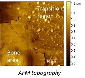
AFSEM image of bone sample with a partially dissolved implant obtained in force volume mode. (Figure 1) AFM Topography image of the bone area and transition region, where the implant is partially dissolved. Image Credit: Quantum Design, Inc.
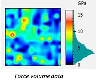
(Figure 2) Force volume data of the same area. Image Credit: Quantum Design, Inc.
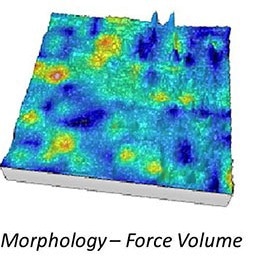
(Figure 3) Overlay of topography and force volume data. Image Credit: Quantum Design, Inc.
C-AFM
A conductive tip is used in the Conductive AFM mode (C-AFM) to evaluate the sample’s conductive characteristics. Focused Electron Beam beam-induced deposition (FEBID) is utilized to create the conductive tips AFSEM uses. They are composed entirely of platinum, guaranteeing their great stability and durability. For C-AFM measurements, no additional module is required.
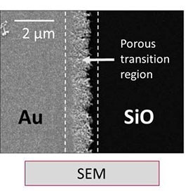
AFSEM C-AFM image of a gold electrode on a silicon substrate. (Figure 1) SEM image of the region of interest displaying the gold electrode with a porous transition region at the edge of the electrode structure. Image Credit: Quantum Design, Inc.
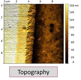
(Figure 2) AFM Topography image of the electrode structure. Image Credit: Quantum Design, Inc.
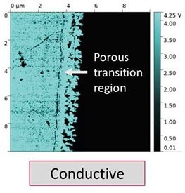
(Figure 3) C-AFM image of the electrode structure that reveals the highly conducting gold electrode as well as the non-conducting silicon surface region. Image Credit: Quantum Design, Inc.
MFM
Using a magnetic tip, MFM is used to investigate the magnetic characteristics of magnetic materials. FEBID is utilized to create the conductive tips required by AFSEM, which is composed of Fe/Co. AFSEM employs a two-step method: The topography is imaged in the first scan.
The phase shift caused by the magnetic force between the tip and the sample is then detected in a second scan in which the tip moves along the observed topography at a predetermined height above the sample. By default, the AFSEM can operate in this so-called “lift-mode.”
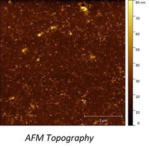
AFSEM MFM image obtained on a multilayered magnetic sample. (Figure 1) AFM Topography. Image Credit: Quantum Design, Inc.
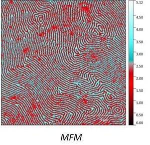
(Figure 2) MFM Phase contrast revealing the different magnetic domains. Image Credit: Quantum Design, Inc.
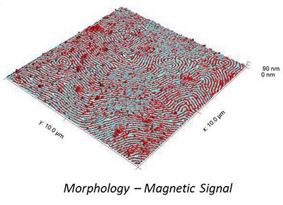
(Figure 3) Overlay of topography and magnetic signal. Image Credit: Quantum Design, Inc.
Download the Brochure for More Information
AFSEM Specifications
AFSEM Nano
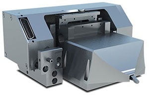
Image Credit: Quantum Design, Inc.
- The smallest AFM insert for the SEM/FIB in the world
- Easy integration in space-constrained areas
- Full-grade V titanium body for optimal mechanical stability and performance
- XY Closed-loop tip-scanner with 24 × 24 µm scan range
- Z-Range: 15 µm
- All standard AFM modes
Videos
AFSEM®nano — Introduction Video
AFSEM®nano — Introduction Video. Video Credit: Quantum Design, Inc.
AFSEM Nanowire Demo
AFSEM Nanowire Demo. Video Credit: Quantum Design, Inc.
AFSEM® I What is your Application?
AFSEM — What is your application?. Video Credit: Quantum Design, Inc.
Download the Brochure for More Information