The Crystal Orientation solutions are crafted to cater to boule, ingot, puck, and wafer applications. The offerings provide straightforward, high-speed crystal orientation across various environments. The company provides users with completely automated online analysis and rapid quality checks.
DDCOM
Ultra-Fast Automated Crystal Orientation in a Compact Package
Precisely ascertain the complete crystal orientation within seconds through the exclusive scanning method. DDCOM demonstrates efficiency with minimal energy consumption and operating costs, making it well-suited for applications in both research and industry.
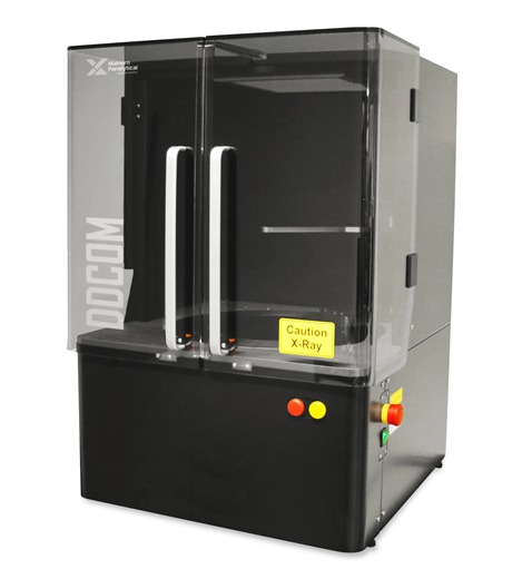
Image Credit: Malvern Panalytical Ltd
Overview
Experience ultra-fast and precise crystal orientation, with accuracy up to 1/100th of a degree at the fingertips. DDCOM delivers dependable results over 100 times faster than conventional methods, further enhancing efficiency through its top-down measurement geometry.
This highly versatile instrument features an air-cooled X-Ray tube and a portable design, ensuring cost-effective operation and maximum convenience. It is an ideal solution for applications such as quality control, marking, and research.
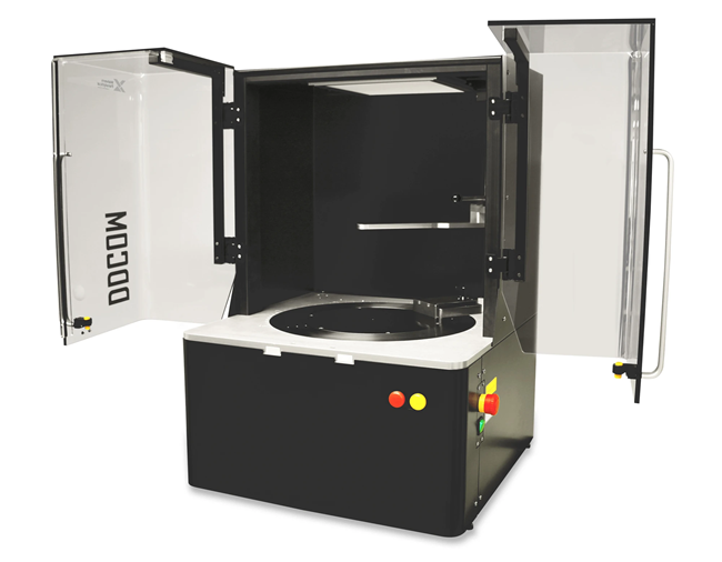
Image Credit: Malvern Panalytical Ltd
Features and Benefits
Ultra-Fast Accuracy
The exclusive scanning technique necessitates just one rotation to collect all essential data for crystal orientation determination, yielding accurate results within 10 seconds (per single rotation).
The instrument’s material-specific geometry allows for the ultra-fast measurement of crystal lattice orientation in relation to the rotation axis, with precision scaling as the number of scan rotations increases.
Compact, User-Friendly Format
DDCOM’s compact design enables seamless integration into any environment. The software, characterized by its combination of power and user-friendly intuitiveness, ensures convenient and straightforward operation for a diverse range of users.
Precise, Efficient Control
Exercise precise control over cutting, grinding, and lapping processes with accuracy up to 1/100th of a degree. DDCOM provides comprehensive lattice orientation data for single crystals and is specifically designed for azimuthal setting and marking of crystal orientation.
Utilizing pre-programmed crystal parameters, the system facilitates the determination of unknown orientations in diverse structures, contributing to the optimization of workflow for enhanced efficiency. Additionally, a range of stage accessories enables metrology at different stages of the process.
Versatile and Cost-Effective
DDCOM is adeptly suited for analysis in both research and production settings, accommodating a variety of sample types. The operational costs for DDCOM remain economical due to its low energy consumption and the utilization of an air-cooled X-Ray tube, eliminating the need for water cooling.
This instrument exhibits versatility by being capable of measuring a diverse range of materials with varying structures, making it a valuable addition to any laboratory. Examples of materials that can be measured include:
- Cubic, arbitrary unknown orientation: Si, Ge, GaAs, GaP, InP
- Cubic, special orientation: Ag, Au, Ni, Pt, GaSb, InAs, InSb, AlSb, ZnTe, CdTe, SiC3C, PbS, PbTe, SnTe, MgO, LiF, MgAl2O4, SrTiO3, LaTiO3
- Hexagonal and trigonal: SiC 2H, 4H, 6H, 15R, GaN, ZnO, LiNbO3, SiO2 (quartz), Al2O3 (sapphire), GaPO4, La3Ga5SiO14
- Tetragonal: MgF2, TiO2, SrLaAlO4
- Orthorhombic: Mg2SiO4, NdGaO3
Key Applications
Crystal Orientation Control for Cutting, Grinding, and Lapping
With its compact design, automation features, and swift measurement capabilities, DDCOM XRD provides a convenient and user-friendly solution for measuring crystal orientation. This allows for precise and efficient control of cutting, grinding, and lapping processes.
Setting and Marking of Crystal Orientation
DDCOM is designed for the azimuthal setting and marking of crystal orientation. The precision and speed required for wafer marking are crucial, and DDCOM provides the necessary swiftness and accuracy for users’ processes. Its lightweight and portable nature allows for easy integration into their current setup or as part of a new process.
Quality Control
Swift measurement speed and efficient throughput are essential for production quality control, and for routine measurements, maintaining low running costs is equally important.
DDCOM excels not only in throughput and productivity, thanks to its top-down measurement geometry, but also in energy efficiency. This ensures that the costs remain low, and the processes run optimally without compromising on quality.
Materials Research
Capable of measuring a diverse array of crystal types within a compact laboratory space, DDCOM is well-suited for standard research workflows. Its operating costs are kept minimal through reduced energy consumption and the use of an air-cooled X-Ray tube, eliminating the need for water cooling.
Additionally, DDCOM is accessible and user-friendly for individuals with varying levels of experience, making it a practical solution for research laboratories.
Specifications
Source: Malvern Panalytical Ltd
| Technical specification |
| X-Ray source |
30 W air-cooled X-Ray tube, Cu anode |
| Detectors |
Two scintillation counters |
| Sample holder |
Precise turntable, setting accuracy 0.01 °, tools for defined sample positioning and marking |
| Physical specification |
| Dimensions |
600 mm × 600 mm × 850 mm |
| Weight |
80 kg |
| Power supply |
100-230 V, 500 W, single phase |
| Room temperature |
≤ 30 °C |
| Configuration options |
| Device for mapping of wafers (maximum diameter 225 mm) |
| Device for automatic loading from cassettes |
| Examples of measurable materials |
| Cubic / arbitrary unknown orientation: Si, Ge, GaAs, GaP, AlAs, AlP, InP, NaCl, AgCl, CaF2 |
| Cubic / special orientation: Ag, Au, Ni, Pt, GaSb, InAs, InSb, AlSb, ZnTe, CdTe, SiC 3C, PbS, PbTe, SnTe, MgO, LiF, MgAl2O4, SrTiO3, LaTiO3 |
| Tetragonal: MgF2, TiO2, SrLaAlO4 |
| Hexagonal / Trigonal: SiC 2H, 4H, 6H, 15R, GaN, ZnO, LiNbO3, SiO2 (quartz), Al2O3 (sapphire), GaPO4, La3Ga5SiO14 |
| Orthorhombic: Mg2SiO4, NdGaO3 |
| Further materials according to the customers’ demands |
SDCOM
Ultra-Fast, Flexible Crystal Orientation in a Compact Package
Capable of measuring crystals with a starting size of 1 mm, the SDCOM employs the azimuthal scan method to accurately ascertain the complete lattice orientation of single crystals in a single measuring rotation, taking just a few seconds.
Versatile and accessible, the SDCOM is suitable for both research and production quality control, seamlessly integrating into various wafer and ingot process steps without the need for water cooling.
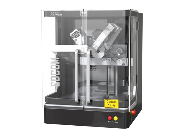
Image Credit: Malvern Panalytical Ltd
Overview
Experience accessible and rapid crystal orientation measurement with the SDCOM, the user-friendly compact XRD solution. Utilizing the azimuthal scan method enables ultra-fast measurements, providing results in under five seconds. The SDCOM ensures the highest level of precision, reaching up to 0.01 °.
With a diverse range of sample holders and transfer fixtures, including a marking option for lateral crystal direction, this easy-to-use compact device is the ideal solution for numerous applications in wafer processing and research.
Features and Benefits
Ultra-Fast and Precise: Azimuthal Scan Method
The azimuthal scan method necessitates just one measuring circle to collect all essential data for a comprehensive orientation determination, offering high precision within a brief measuring time, typically in the range of a few seconds.
During this process, the sample undergoes a 360-degree rotation while the X-Ray source and detector are strategically positioned to achieve a specific number of reflections per turn. These reflections enable the precise measurement of the crystal lattice orientation in relation to the rotation axis, accomplished swiftly and with high accuracy.

Image Credit: Malvern Panalytical Ltd
Compact and Versatile
SDCOM boasts a lightweight and compact design, facilitating easy mobility and seamless integration into the processes, whether in a research or industrial setting. The XRD Suite software, known for its powerful and intuitive features, ensures convenience and user-friendly operation across a diverse user base.
The SDCOM emphasizes flexibility, which is evident in its ability to measure a broad range of materials. Capable of measuring crystals starting from 1 mm in size, it offers versatility in applications. Examples of measurable materials include:
- Cubic, arbitrary unknown orientation: Si, Ge, GaAs, GaP, InP
- Tetragonal: MgF2, TiO2, SrLaAlO4
- Orthorhombic: Mg2SiO4, NdGaO3
- Cubic, special orientation: Ag, Au, Ni, Pt, GaSb, InAs, InSb, AlSb, ZnTe, CdTe, SiC3C, PbS, PbTe, SnTe, MgO, LiF, MgAl2O4, LaTiO3, SrTiO3,
- Hexagonal and trigonal: SiC 2H, 4H, 6H, 15R, GaN, ZnO, LiNbO3, SiO2 (quartz), Al2O3 (sapphire), GaPO4, La3Ga5SiO14
Additionally, a diverse array of sample holders and transfer fixtures is available to broaden the applications of users’ SDCOM, ensuring seamless compatibility with their workflow. Both manual and motorized wafer mapping stages are also at their disposal.

Image Credit: Malvern Panalytical Ltd
User-Friendly Precision
SDCOM achieves outstanding precision, reaching up to 0.01 degrees, dependent on the sample, and is capable of measuring crystals ranging from 1 mm and larger.
This high precision is sustained at top speeds, courtesy of the azimuthal scan method, offering comprehensive characterization of crystal orientation in a single measuring rotation. Additionally, there is an option to incorporate a lateral crystal direction marking function.
The SDCOM is user-friendly and easily accessible, thanks to manual handling and an intuitively designed software interface. This practicality makes it suitable for use in both research and industry, accommodating varying levels of user experience.

Image Credit: Malvern Panalytical Ltd
Cost-Effective
The X-Ray tube in SDCOM is air-cooled, eliminating the necessity for water cooling. The efficiency and compact design of SDCOM contribute to minimal energy consumption, thereby keeping your operational costs to a minimum.

Image Credit: Malvern Panalytical Ltd
Key Applications
Marking and Measuring In-Plane Directions
SDCOM provides rapid and exceptionally accurate crystal orientation measurements, making it ideal for various applications in wafer production and processing, including marking and measuring in-plane directions. Its lightweight and portable design enables deployment wherever needed in the process.
With the ability to measure small crystals down to 1 mm with high precision and accommodate a diverse range of materials, SDCOM is well-suited to meet the dynamic and intricate requirements of the semiconductor industry.
Production Quality Control
Routine process control requires speed, precision, and repeatability, all of which SDCOM delivers. Its ultra-fast measurement speed enhances productivity without significantly affecting running costs, thanks to its desktop format and air-cooled X-Ray tube.
Materials Research
Capable of measuring a diverse range of crystal types within a compact laboratory space, SDCOM is well-suited for standard research workflows.
Its running costs remain low due to minimized energy consumption and an air-cooled X-Ray tube that eliminates the need for water cooling. SDCOM is also user-friendly and easily accessible with manual handling, making it a practical solution for research laboratories with a diverse user base.
Specifications
Source: Malvern Panalytical Ltd
| . |
. |
| X-Ray source |
30 W air-cooled X-Ray tube, Cu anode |
| Detectors |
Scintillation counter technology |
| Sample holder |
Precise turntable, setting accuracy 0.01 °, customized sample holders, and transfer fixtures |
| Sample diameter |
Down to 2 mm ø, up to 200 mm |
| Ambient temperature |
≤ 30 °C |
| PC requirements |
Windows 10 or latest, . NET Framework update, 2 Ethernet ports |
| Power requirements |
100 to 230 V, single phase, 500 W |
| Dimensions |
600 mm (L) x 600 mm (B) x 840 mm (H) |
| Weight |
ca, 100 kg |
| Certification |
Manufactured under ISO 9001 guidelines, CE conform |
| All technical parameters are subject to changes based on R&D |
Omega/Theta XRD
Fully Automated Vertical Three-Axes X-Ray Diffractometer for Ultra-Fast Crystal Orientation
The Omega/Theta XRD achieves an unparalleled combination of precision and speed in determining crystal lattice orientation.
Providing results in as little as ten seconds, this XRD system comes equipped with various process accessories, including barcode readers and crystal stacking frames.
It can handle a diverse range of samples, accommodating weights of up to 30 kg and lengths of up to 450 mm. As a dependable partner, it facilitates the transfer of measured orientation data to the users’ processing tool.
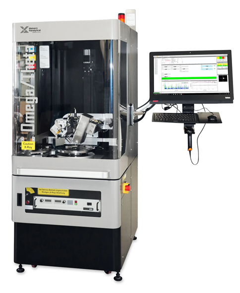
Image Credit: Malvern Panalytical Ltd
Overview
The Omega/Theta XRD stands as the steadfast and future-proof ally for determining crystal orientation in the ever-evolving semiconductor landscape. It blends market-leading precision, rapid measurement speed, and top-notch build quality with the strength of automation, ensuring the processes remain adaptable.
With unmatched efficiency and precision for crystal orientation and alignment, the Omega/Theta XRD proves ideally suited for both production and research applications.
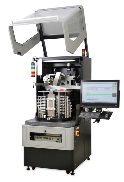
Image Credit: Malvern Panalytical Ltd
Features and Benefits
Ultra-Fast Precision With Proprietary Scan Technology
The approach necessitates just one measuring circle to collect all the essential data for a comprehensive orientation determination, ensuring high precision within a very brief measuring time—typically in the range of a few seconds.
Easy Interfacing for Advanced Connectivity and Automated Measurements
All measurements conducted on the Omega/Theta XRD are automated and controlled through the user-friendly XRD software. The instrument seamlessly integrates into existing production processes in production environments, utilizing its diverse MES, SECS/GEM, and similar interfaces.
Characterize a Range of Materials
Omega/Theta XRD is applicable for characterizing all single-crystalline materials. Some commonly utilized materials include:
- Si
- Ge
- GaN
- GaAs
- AIN
- SiC
- CdTe
- BBO
- LiNbO3
- Quartz
Convenient, Flexible Sample Handling
The extensive array of accessories boosts the productivity of the Omega/Theta XRD across a broad spectrum of applications, ranging from seed boring and grinding to slicing and wafer geometry end control. This ensures flexibility, even as user needs evolve over time. Additional components include:
- Automatic X-Y mapping stage for mapping crystal orientation or surface distortions on a user-defined grid
- Rocking curve tool for quality measurement
- Additional sample rotation axis
- Stacking stage for aligning ingots before sawing
- Photographic camera and image processing
- Sample adjustment equipment
- Numerous other custom engineering solutions!
- Laser scanner for sample shape measurement
Featuring tailored sample holders designed to fulfill requirements ranging from large ingots to tiny cylinders, the Omega/Theta XRD can adapt to a diverse array of sample sizes. This versatility ensures its seamless integration into both production workflows and research environments.
Key Applications
Production
Crafted with manufacturers in mind, the Omega/Theta XRD excels in the rapid orientation and alignment of diverse crystal types within production processes. Whether marking in-plane directions or verifying the orientation of flats or notches, it proves ideal for production quality control, offering high throughput speeds and automation capabilities.
Optional extras, such as a stacking stage for aligning ingots before sawing and a rocking curve tool for quality measurements, further enhance the versatility of the Omega/Theta XRD as a reliable partner for production applications.
Materials Research
The Omega/Theta XRD, known for its high precision and flexibility, proves ideal for materials research. It can accommodate samples up to 30 kg and 450 mm in length, with additional stages available for larger or more complex samples. With the capability to characterize a diverse range of materials, it becomes highly valuable for users’ R&D processes. The flexible Theta Scan functionality further expands the realm of measurement possibilities.
Specification
Source: Malvern Panalytical Ltd
| Technical specification |
| X-Ray source |
Standard X-Ray tube, Cu anode |
| Detector |
Scintillation counter (single or double) |
| Sample holder |
Precise turntable, mounting plate, and tools for sample adjustment |
| Crystal collimator |
Available |
| Mapping |
Heavy duty mapping stage available |
| Software |
XRDStudio |
| Water cooling |
Flow – 4 l/min, max. pressure 8 bar, T ≤ 30 °C |
| PC workstation |
Windows 7 or latest, .NET Framework update |
| Dimensions |
H 1950 mm × D 820 mm × W 1200 mm |
| Weight |
ca, 650 kg |
| Power requirement |
208-240 V, 16 A single phase, 50-60 Hz |
| Certification |
Manufactured under ISO 9001 guidelines, CE conform |
Wafer XRD 200
Fast, Precise, and Fully Equipped: The Solution for Wafer End Control
Wafer XRD 200 stands as an ultra-fast, high-precision automated system designed for wafer sorting based on crystal orientation and wafer geometry parameters. It comes equipped with a multitude of additional options to enhance its functionality.
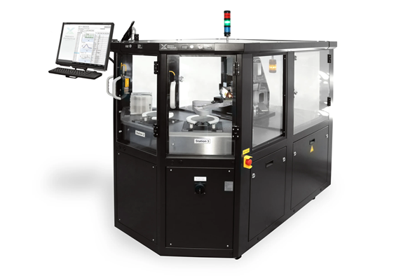
Image Credit: Malvern Panalytical Ltd
Overview
Wafer XRD 200 is a fully automated, high-speed X-Ray diffraction platform revolutionizing wafer production and research.
It delivers crucial data on essential parameters such as crystal orientation, resistivity, geometric features (notches and flats), distance measurements, and more, all within a matter of seconds. Engineered to seamlessly integrate into the process line, Wafer XRD 200 offers unparalleled efficiency.
Features and Benefits
Ultra-Fast Precision With Proprietary Scan Technology
The method necessitates just one rotation of the wafer to collect all the essential data for a comprehensive orientation determination. This results in high precision achieved within a very brief measuring time, typically in the range of a few seconds.
Fully Automated Handling and Sorting
Engineered to enhance users’ throughput and productivity, Wafer XRD 200 features full automation for handling and sorting. With detailed data transmission tools, this device becomes a powerful and efficient element in their quality control process.

Image Credit: Malvern Panalytical Ltd
Easy Connectivity
The robust automation of Wafer XRD 200 is compatible with both MES and SECS/GEM interfaces, allowing it to seamlessly integrate into the new or existing process.

Image Credit: Malvern Panalytical Ltd
High Precision, Deeper Insight
Gain unprecedented insights into the materials with the key measurements provided by Wafer XRD 200. It measures:
- Crystal orientation
- Notch position, depth, and opening angle
- Diameter
- Flat position and length
- Resistivity
The typical standard deviation tilt (illustration: Si 100) for the Azimuthal-scan is <0.003 °, with a minimum of <0.001 °.
Powerful and Versatile
The Wafer XRD 200 facilitates a diverse range of measurements at high speed, adding substantial value to the processes, be it in research or production. However, its versatility and flexibility extend beyond just speed.
Wafer XRD 200 simplifies and accelerates the analysis of hundreds of potential samples, encompassing:
- Si
- SiC
- Quartz
- AlN
- Al2O3 (sapphire)
- LiNbO3
- GaAs
- BBO
Key Applications
Production and Processing
In this dynamic industry where speed is crucial, automation becomes a necessity, and the Wafer XRD 200 takes the lead as a pragmatic and potent solution for handling wafers, sorting, and conducting in-depth measurements.
It covers critical aspects such as crystal orientation, optical notch and flat determination, resistivity measurements, and other essential parameters. Witness the enhanced productivity firsthand.
Quality Control
Accurate and rapid comprehension of the materials is pivotal for effective quality control, and the Wafer XRD 200 stands out as the optimal solution.
Employing the ultra-fast Omega-Scan method, it discerns crystal orientation in a single measurement, delivering results within 5 seconds. With added features, such as resistivity measurement and geometric feature determination, the Wafer XRD 200 provides unmatched efficiency and versatility for production quality control.
Materials Research
Busy environments are not limited to production settings—Wafer XRD 200 is well-equipped to offer high-throughput analysis in both R&D environments.
Capable of characterizing a vast array of materials, from Si, SiC, and GaAs to quartz, LiNbO3, and BBO, the Wafer XRD 200 possesses the versatility to aid in materials research and innovation, playing a role in shaping the future of semiconductor technology.
Specifications
Source: Malvern Panalytical Ltd
| . |
. |
| Throughput |
10000+ Wafer per Month |
| Wafer geometry |
On request |
| Tilt precision |
0.003 |
| XRD axis vs notch / flat position |
0.03 ° |
Wafer XRD 300
The Integratable Wafer Orientation Solution
Harness the potential of factory automation with cutting-edge X-Ray diffraction technology. The Wafer XRD 300 stands as an ultra-fast, high-precision metrology module designed for crystal orientation and wafer geometry control.
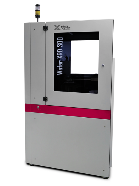
Image Credit: Malvern Panalytical Ltd
Overview
Introducing the Wafer XRD 300: a high-speed X-Ray diffraction module tailored for 300 mm wafer production, offering crucial data on essential parameters like crystal orientation and geometric features including notches, flats, and more. Engineered to seamlessly integrate into the process line.
Features and Benefits
Ultra-Fast Precision With the Proprietary Scan Technology
The employed method necessitates just a single rotational scan to collect all essential data, enabling a comprehensive determination of crystal orientation with high precision within a very brief measuring time—typically in the range of a few seconds.
Fully Automated Handling and Sorting
Wafer XRD 300 is crafted to optimize throughput and productivity. Seamless integration into the handling and sorting automation renders it a potent and efficient addition to the process.

Image Credit: Malvern Panalytical Ltd
Easy Connectivity
The robust automation of Wafer XRD 300 seamlessly integrates into the new or existing process, offering compatibility with both MES and SECS/GEM interfaces.

Image Credit: Malvern Panalytical Ltd
High Precision, Deeper Insight
Gain unparalleled insights into the materials with Wafer XRD 300's crucial measurements, including:
- Crystal orientation
- Notch position, depth, and opening angle
- Diameter
- Flat position and length
- Additional sensors available upon request
The standard deviation tilt (for example, Si 100) in the Azimuthal-scan typically falls below <0.003 °.
Powerful and Versatile
As semiconductor research evolves, it has never been more important to measure a variety of samples. Wafer XRD 300 makes analysis easy and fast for hundreds of materials, including:
- Si
- SiC
- AlN
- GaAs
- Quartz
- Al2O3 (sapphire)
- LiNbO3
- BBO
Key Applications
Production and Processing
The Wafer XRD 300 is at the forefront of the transformation brought about by advancements in automation, offering a pragmatic and potent solution for managing orientation measurements at unprecedented speeds.
Quality Control
Wafer XRD 300 provides unmatched efficiency and versatility for production quality control, delivering highly accurate results in under 10 seconds. Tailored for 300 mm production environments, it excels in seamless integration into custom automation setups.
Specifications
Source: Malvern Panalytical Ltd
| . |
. |
| Throughput |
10000+ Wafer per Month |
| Wafer geometry |
On request |
| Tilt precision |
0.003 |
| XRD axis vs notch / flat position |
0.03 ° |
XRD-OEM
Fully Automated In-Line Orientation and Handling of Ingots, Boules, and Pucks
The dedicated solution for automated in-line handling, machining, and measurement of ingots, boules, and panels. XRD-OEM is designed for peak performance even in the most challenging environments.
XRD-OEM is a resilient solution that enhances productivity, ensures quality control, and optimizes your production processes.
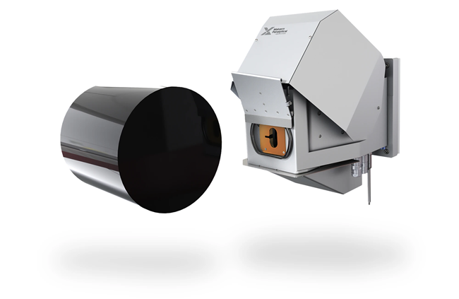
Image Credit: Malvern Panalytical Ltd
Overview
XRD-OEM stands as a transformative force for the production processes. Engineered to endure the demanding conditions of grinding and sawing, this X-Ray diffraction instrument seamlessly integrates with any processing system, thanks to its industry-standard interfacing.
XRD-OEM delivers independent orientation measurements for ingots, boules, or panels, facilitating measurements on both flat surfaces and circumferences. Optical notch detection ensures precise pre-alignment before the sawing or grinding processes.
Features and Benefits
Compact and Connected
Tailored for seamless integration with any automation or processing system, XRD-OEM facilitates a streamlined, efficient, and uninterrupted operation.
Its compact design and standard industrial interfaces guarantee easy incorporation into any manufacturing setup, ensuring compatibility with the existing instruments and systems.
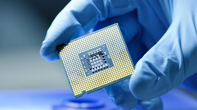
Image Credit: Malvern Panalytical Ltd
Tough Enough for the Process
Crafted for durability, XRD-OEM is deployable in any environment you require, including grinding and sawing processes. It remains reliable and precise, maintaining performance even under demanding production conditions.
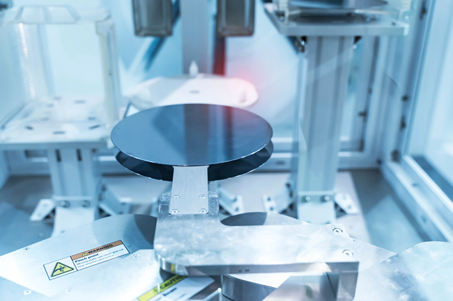
Image Credit: Malvern Panalytical Ltd
Fast and Precise
XRD-OEM provides automated precision where it is most crucial. The accurate determination of crystal orientation upholds stringent quality control standards, optimizing the processes for increased efficiency and overall quality.
XRD-OEM excels in determining crystal orientation on both flat surfaces and circumferences, adding an extra layer of versatility.
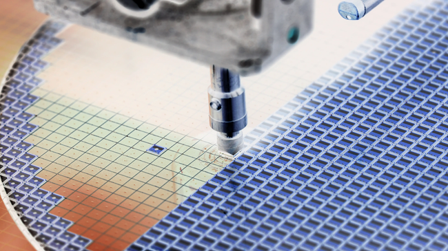
Image Credit: Malvern Panalytical Ltd
Optical Notch Detection
Optical notch detection precisely identifies and characterizes flat and notch features on the samples, playing a crucial role in the pre-alignment of large ingots before the sawing or grinding processes.
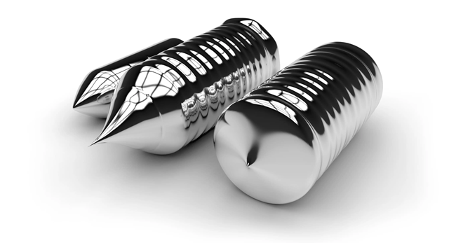
Image Credit: Malvern Panalytical Ltd
Wide Range of Sample Sizes
XRD-OEM can determine crystal orientation on both flat surfaces and circumferences, adding an extra layer of versatility.

Image Credit: Malvern Panalytical Ltd
Key Applications
Production and Processing
Tailored for users bustling production environment, XRD-OEM is crafted as an in-line instrument, ready to seamlessly integrate into the automated high-throughput setup. It serves as an efficient solution for measuring and handling ingots, boules, and panels.
With the capability to measure a variety of compound semiconductor materials, including Si, SiC, GaAs, and more, its air-cooling and compact size make it a potent and cost-effective addition to their process.
Ingot Pre-Alignment Before Sawing or Grinding
Through its precise pre-alignment capabilities, XRD-OEM facilitates accurate positioning and orientation control before advancing to subsequent processing steps.
Quality Control
In the realm of production, swift orientation measurements are imperative, and XRD-OEM excels in delivering high-quality data with speed. By seamlessly integrating into both new and existing automated processes, XRD-OEM positions users to embrace the automated future of manufacturing today.
Specifications
Source: Malvern Panalytical Ltd
| . |
. |
| Notch position |
0.005 ° |
| Notch depth |
0.005 mm |
| Notch profile angle, typical |
< 0.5 ° |
| Diameter |
0.02 mm |
| Flat position |
< 0.03 ° |
| Flat length |
< 0.3 mm |