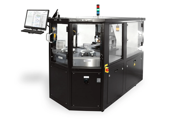
Wafer XRD 200
Fast, Precise, and Fully Equipped: The Solution for Wafer End Control
Wafer XRD 200 stands as an ultra-fast, high-precision automated system designed for wafer sorting based on crystal orientation and wafer geometry parameters. It comes equipped with a multitude of additional options to enhance its functionality.

Image Credit: Malvern Panalytical Ltd
Overview
Wafer XRD 200 is a fully automated, high-speed X-Ray diffraction platform revolutionizing wafer production and research.
It delivers crucial data on essential parameters such as crystal orientation, resistivity, geometric features (notches and flats), distance measurements, and more, all within a matter of seconds. Engineered to seamlessly integrate into the process line, Wafer XRD 200 offers unparalleled efficiency.
Features and Benefits
Ultra-Fast Precision With Proprietary Scan Technology
The method necessitates just one rotation of the wafer to collect all the essential data for a comprehensive orientation determination. This results in high precision achieved within a very brief measuring time, typically in the range of a few seconds.
Fully Automated Handling and Sorting
Engineered to enhance users’ throughput and productivity, Wafer XRD 200 features full automation for handling and sorting. With detailed data transmission tools, this device becomes a powerful and efficient element in their quality control process.

Image Credit: Malvern Panalytical Ltd
Easy Connectivity
The robust automation of Wafer XRD 200 is compatible with MES like SECS/GEM, allowing it to seamlessly integrate into the new or existing process.

Image Credit: Malvern Panalytical Ltd
High Precision, Deeper Insight
Gain unprecedented insights into the materials with the key measurements provided by Wafer XRD 200. It measures:
- Crystal orientation
- Notch position, depth, and opening angle
- Diameter
- Flat position and length
- Resistivity
The typical standard deviation tilt (illustration: Si 100) for the Azimuthal-scan is <0.003 °, with a minimum of <0.001 °.
Wafer XRD 200 simplifies and accelerates the analysis of hundreds of potential samples, encompassing:
- Si
- SiC
- Quartz
- AlN
- Al2O3 (sapphire)
- LiNbO3
- GaAs
- BBO
Key Applications
Production and Processing
In this dynamic industry where speed is crucial, automation becomes a necessity, and the Wafer XRD 200 takes the lead as a potent solution for handling wafers, sorting, and conducting in-depth measurements.
It covers critical aspects such as crystal orientation, optical notch and flat determination, resistivity measurements, and other essential parameters. Witness the enhanced productivity firsthand.
Quality Control
Accurate and rapid comprehension of the materials is pivotal for effective quality control, and the Wafer XRD 200 stands out as the optimal solution.
Employing the ultra-fast Omega-Scan method, it discerns crystal orientation in a single measurement, it can measure up to 1 million wafers per year. With optional features, such as resistivity measurement and geometric feature determination, the Wafer XRD 200 provides unmatched efficiency and versatility for production quality control.
Materials Research
Busy environments are not limited to production settings—Wafer XRD 200 is well-equipped to offer high-throughput analysis in R&D environments.
Capable of characterizing a vast array of materials, from Si, SiC, and GaAs to quartz, LiNbO3, and BBO, the Wafer XRD 200 possesses the versatility to aid in materials research and innovation, playing a role in shaping the future of semiconductor technology.
Specifications
Source: Malvern Panalytical Ltd
| . |
. |
| Throughput |
10000+ Wafer per Month |
| Wafer geometry |
On request |
| Tilt precision |
0.003 |
| XRD axis vs notch / flat position |
0.03 ° |